
Page 150 - Sensors and Control Systems in Manufacturing
P. 150
Classification and Types of Sensors
FIGURE 2.105 Images (generated by Hyphenated Systems) of advanced confocal 111
profi ling systems provide the same height information available from scanning-
electron microscope (SEM) cross-section measurements.
The probe mark is relatively shallow, with the deepest portion
less than 500 nm below the pad level.
The mark is deeper and clearly shows a breakthrough to a barrier
layer and the underlying dielectric around 1 µm beneath the pad sur-
face. (Courtesy of Hyphenated Systems.)
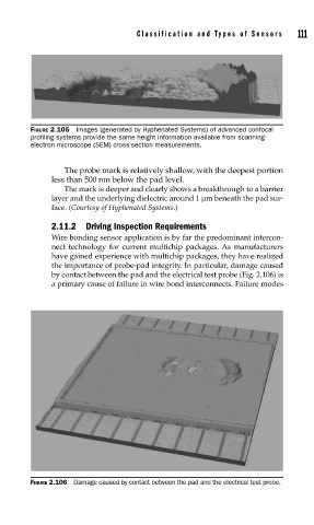
2.11.2 Driving Inspection Requirements
Wire bonding sensor application is by far the predominant intercon-
nect technology for current multichip packages. As manufacturers
have gained experience with multichip packages, they have realized
the importance of probe-pad integrity. In particular, damage caused
by contact between the pad and the electrical test probe (Fig. 2.106) is
a primary cause of failure in wire bond interconnects. Failure modes
FIGURE 2.106 Damage caused by contact between the pad and the electrical test probe.