
Page 151 - Sensors and Control Systems in Manufacturing
P. 151
112
T w o
Cha p te r
include excessive marking, which interferes with the bond reliability;
punch-through, which reduces bond reliability and exposes underly-
ing circuitry to the bonding process; and etch defects, in which over-
lying passivation is not completely cleared from the bond pad.
Another issue of growing importance is vendor accountability.
Many devices incorporate chips from different vendors. Corporate
integrators do not desire to be held responsible for defects that
occurred upstream in the supply chain, and many are implementing
incoming probe-mark inspection or imposing requirements for out-
going inspection on their suppliers, or both.
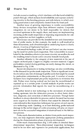
Microscopy can provide for the detailed review and characteriza-
tion of probe marks. In this example, the mark is well resolved in
three dimensions, and a breakthrough to underlying layers is clearly
shown. (Courtesy of Hyphenated Systems.)
Advanced technology nodes (65 nm and below) are also increas-
ing the need for probe-mark inspection. This vulnerability is exacer-
bated by the relentless efforts to put more circuitry on smaller die and
the resulting trend to locate active circuitry beneath bond pads.
Another offender in the category of new materials is the use of
copper on bond pads. Copper is a highly corrosive material. Copper
particulates created during probing can easily damage the circuit, as
illustrated in Fig. 2.106.
Recent developments in testing technology are also contributing
to the demand for probe-mark inspection. There is significant incen-
tive to reduce any risk of damage to probe cards that might be caused
by particulate contaminants on the probe pad. A number of manu-
facturers have implemented pre-probe inspections to minimize this
risk. Probes wear during normal use but may be reconditioned or
repaired up to a certain point. Careful analysis of probe marks can
provide information that signals the need for reconditioning of a
probe.
Another trend in test technology is the movement of electrical
testing upstream, into the fabrication process, to allow faster detec-
tion, diagnosis, and correction of defective processes. Though faster
feedback is always desirable for process control, the need has become
more urgent as the fraction of defects that cannot be detected with
conventional in-line inspection techniques has grown at each succes-
sive technology node. Limiting, or at least detecting, probe-induced
damage in the earlier stages of wafer processing will play an impor-
tant role in the successful integration of electrical tests in the fabrica-
tion process.
Probe-mark characterization, as distinct from probe-mark inspec-
tion, can help engineers determine appropriate probing parameters
during the characterization phase of process development.
Probe-mark characterization (Fig. 2.105) relies on detailed three-
dimensional inspection. Three-dimensional inspection techniques
tend to be too slow and expensive for production applications, but