
Page 89 - Understanding Automotive Electronics
P. 89
2735 | CH 3 Page 76 Tuesday, March 10, 1998 11:03 AM
3 ELECTRONICS FUNDAMENTALS
dotted resistance in parallel with the collector-base diode represents the leakage
of the reverse biased junction, which is normally neglected, as discussed
previously.
A transistor is saturated A third condition known as the saturation condition exists under certain
when a large increase in conditions of collector-emitter voltage and collector current. In the saturation
the base-to-emitter cur- condition, large increases in the transistor base current produce little increase in
rent results in only a collector current. When saturated, the voltage drop across the collector-emitter
small increase in the col- is very small, usually less than 0.5 volt. This is the on condition for a transistor
lector current. switching circuit. This condition occurs in a switching circuit when the
collector of the transistor is tied through a resistor R to a supply voltage V as
c
L
shown in Figure 3.2c. Enough base current is supplied to the transistor to drive
the transistor into the saturated condition, in which the output voltage (voltage
drop from collector to emitter) is very small and the collector-base diode may
become forward biased. Having briefly described the behavior of transistors, it
is now possible to discuss circuit applications for them.
TRANSISTOR AMPLIFIERS
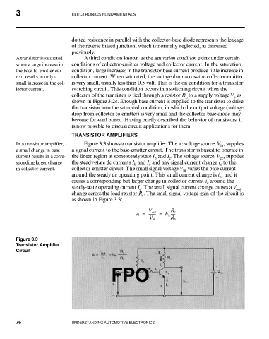
In a transistor amplifier, Figure 3.3 shows a transistor amplifier. The ac voltage source, V , supplies
in
a small change in base a signal current to the base-emitter circuit. The transistor is biased to operate in
current results in a corre- the linear region at some steady state I and I . The voltage source, V , supplies
b c cc
sponding larger change the steady-state dc currents I and I and any signal current change i to the
b c c
in collector current. collector-emitter circuit. The small signal voltage V varies the base current
in
around the steady dc operating point. This small current change is i , and it
b
causes a corresponding but larger change in collector current i around the
c
steady-state operating current I . The small signal current change causes a V
c out
change across the load resistor R . The small signal voltage gain of the circuit is
c
as shown in Figure 3.3:
V out R c
A = -------- = h fe -----
V in R b
Figure 3.3
Transistor Amplifier
Circuit
FPO
76 UNDERSTANDING AUTOMOTIVE ELECTRONICS