
Page 97 - Understanding Automotive Electronics
P. 97
2735 | CH 3 Page 84 Tuesday, March 10, 1998 11:03 AM
3 ELECTRONICS FUNDAMENTALS
Digital circuit operation is represented in terms of logical variables that
are denoted here with capital letters. For example, in the next few sections A, B,
and C represent logical variables that can have a value of either 0 or 1.
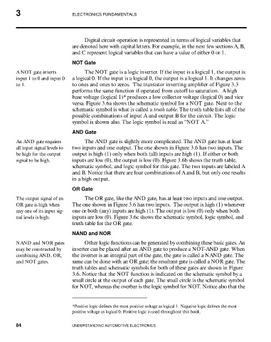
NOT Gate
A NOT gate inverts The NOT gate is a logic inverter. If the input is a logical 1, the output is
input 1 to 0 and input 0 a logical 0. If the input is a logical 0, the output is a logical 1. It changes zeros
to 1. to ones and ones to zeros. The transistor inverting amplifier of Figure 3.3
performs the same function if operated from cutoff to saturation. A high
base voltage (logical 1)* produces a low collector voltage (logical 0) and vice
versa. Figure 3.6a shows the schematic symbol for a NOT gate. Next to the
schematic symbol is what is called a truth table. The truth table lists all of the
possible combinations of input A and output B for the circuit. The logic
symbol is shown also. The logic symbol is read as “NOT A.”
AND Gate
An AND gate requires The AND gate is slightly more complicated. The AND gate has at least
all input signal levels to two inputs and one output. The one shown in Figure 3.6 has two inputs. The
be high for the output output is high (1) only when both (all) inputs are high (1). If either or both
signal to be high. inputs are low (0), the output is low (0). Figure 3.6b shows the truth table,
schematic symbol, and logic symbol for this gate. The two inputs are labeled A
and B. Notice that there are four combinations of A and B, but only one results
in a high output.
OR Gate
The output signal of an The OR gate, like the AND gate, has at least two inputs and one output.
OR gate is high when The one shown in Figure 3.6 has two inputs. The output is high (1) whenever
any one of its input sig- one or both (any) inputs are high (1). The output is low (0) only when both
nal levels is high. inputs are low (0). Figure 3.6c shows the schematic symbol, logic symbol, and
truth table for the OR gate.
NAND and NOR
NAND and NOR gates Other logic functions can be generated by combining these basic gates. An
may be constructed by inverter can be placed after an AND gate to produce a NOT-AND gate. When
combining AND, OR, the inverter is an integral part of the gate, the gate is called a NAND gate. The
and NOT gates. same can be done with an OR gate; the resultant gate is called a NOR gate. The
truth tables and schematic symbols for both of these gates are shown in Figure
3.6. Notice that the NOT function is indicated on the schematic symbol by a
small circle at the output of each gate. The small circle is the schematic symbol
for NOT, whereas the overbar is the logic symbol for NOT. Notice also that the
*Positive logic defines the most positive voltage as logical 1. Negative logic defines the most
positive voltage as logical 0. Positive logic is used throughout this book.
84 UNDERSTANDING AUTOMOTIVE ELECTRONICS