
Page 61 - Wire Bonding in Microelectronics
P. 61
40 Cha pte r T w o
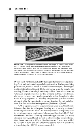
FIGURE 2-18 Photograph of devices bonded with large Al ribbon [80 × 8 mil
(2 × 0.2 mm)], using a waffl e pattern ultrasonic bonding tool. The upper
picture is taken directly from the top and clearly reveals the patterned tool,
and how such bonding can be oriented to connect die or pads that are displaced
from a straight line. Lower fi gure is tipped to show the stress-relief looping
between bonds. (Courtesy of Orthodyne Electronics.)
Pt wire work-hardens significantly during cold ultrasonic wedge bond-
ing. So, it is often bonded by parallel-gap (electrical discharge) welding
[2-66 to 2-68], which is a form of thermocompression (TC) bonding (no
melting takes place). Figure 2-19 shows a typical setup for parallel gap
welding. Platinum has a high resistivity and low thermal conductivity,
which are helpful properties for this welding method. The electrical
discharge, between two closely spaced electrodes through the wire,
heats it to appropriate TC bonding temperatures (several hundred
degrees), while the clamping force presses it against the pad metalliza-
tion. This forms the thermocompression (deformation) bond.
PGW is typically used for larger diameter wires [e.g., ≥100 (4 mil)].
It is not adaptable for high-speed bonding and is usually performed
manually, one wire at a time. This bonding method is frequently used
in high-temperature electronics. Johnson and Fendrock [2-67, 2-68]
describe the methods of setting the bonding parameters (i.e., force,
electrical power, and time), as well as other welding setup informa-
tion. In one example, a 125 µm (5 mil) diameter Pt wire was welded
to a 0.5 µm Pt bond pad on a sapphire substrate. For such situations,
a heated stage (at ~200°C) was recommended.