
Page 65 - Wire Bonding in Microelectronics
P. 65
44 Cha pte r T w o
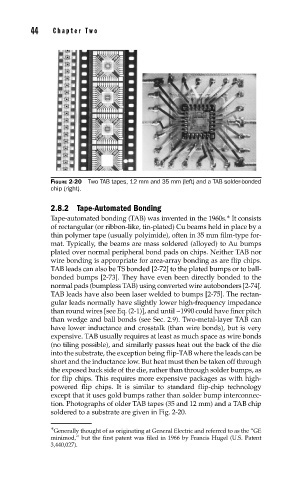
FIGURE 2-20 Two TAB tapes, 12 mm and 35 mm (left) and a TAB solder-bonded
chip (right).
2.8.2 Tape-Automated Bonding
Tape-automated bonding (TAB) was invented in the 1960s. ∗ It consists
of rectangular (or ribbon-like, tin-plated) Cu beams held in place by a
thin polymer tape (usually polyimide), often in 35 mm film-type for-
mat. Typically, the beams are mass soldered (alloyed) to Au bumps
plated over normal peripheral bond pads on chips. Neither TAB nor
wire bonding is appropriate for area-array bonding as are flip chips.
TAB leads can also be TS bonded [2-72] to the plated bumps or to ball-
bonded bumps [2-73]. They have even been directly bonded to the
normal pads (bumpless TAB) using converted wire autobonders [2-74].
TAB leads have also been laser welded to bumps [2-75]. The rectan-
gular leads normally have slightly lower high-frequency impedance
than round wires [see Eq. (2-1)], and until ~1990 could have finer pitch
than wedge and ball bonds (see Sec. 2.9). Two-metal-layer TAB can
have lower inductance and crosstalk (than wire bonds), but is very
expensive. TAB usually requires at least as much space as wire bonds
(no tiling possible), and similarly passes heat out the back of the die
into the substrate, the exception being flip-TAB where the leads can be
short and the inductance low. But heat must then be taken off through
the exposed back side of the die, rather than through solder bumps, as
for flip chips. This requires more expensive packages as with high-
powered flip chips. It is similar to standard flip-chip technology
except that it uses gold bumps rather than solder bump interconnec-
tion. Photographs of older TAB tapes (35 and 12 mm) and a TAB chip
soldered to a substrate are given in Fig. 2-20.
∗
Generally thought of as originating at General Electric and referred to as the “GE
minimod,” but the first patent was filed in 1966 by Francis Hugel (U.S. Patent
3,440,027).