Page 158 - A Comprehensive Guide to Solar Energy Systems
P. 158
Chapter 8 • Photovoltaics: The Basics  159


                 where D n  and D p  are diffusion coefficients of electrons and holes, respectively. diffusion
                 coefficients are connected with electron and hole mobility by D n  = kTµ n /q, D p  = kTµ p /q
                                    −1
                 (k = 1.381 × 10 −23  J K  is the Boltzmann constant). details describing influence of tem-
                 perature and doping concentration on the carrier mobility in crystalline silicon can be
                 found in [4].
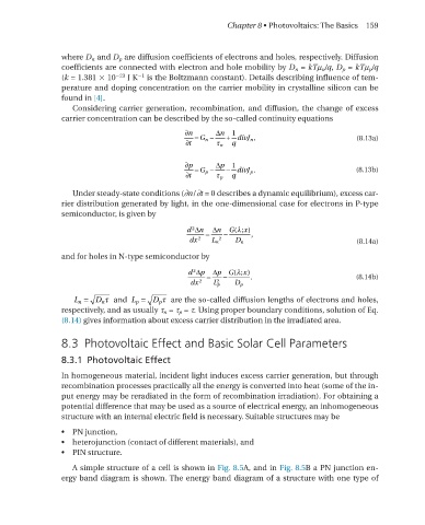
                   Considering carrier generation, recombination, and diffusion, the change of excess
                 carrier concentration can be described by the so-called continuity equations
                                                ∂n    −  ∆n +  1  divJ ,                   (8.13a)
                                                ∂t  = G n  τ n  q  n                                                                       ∂n∂t=Gn−∆nτn+1qdivJn,


                                                            1
                                                ∂p    −  ∆p  − divJ .                      (8.13b)
                                                ∂t  = G p  τ p  q  p                                                                       ∂p∂t=Gp−∆pτp−1qdivJp.
                   under steady-state conditions (∂n/∂t = 0 describes a dynamic equilibrium), excess car-
                 rier distribution generated by light, in the one-dimensional case for electrons in P-type
                 semiconductor, is given by

                                                             λ x)
                                                d 2 ∆n  =  ∆n  −  G(;  ,
                                                 dx 2  L n 2  D n                          (8.14a)                                         d ∆ndx =∆nLn −G(λ;x)Dn,
                                                                                                                                                 2
                                                                                                                                             2
                                                                                                                                                       2
                 and for holes in n-type semiconductor by
                                                             λ x)
                                                 d 2 ∆p  =  ∆p  −  G(;  .                  (8.14b)
                                                 dx 2  L p 2  D p                                                                          d ∆pdx =∆pLp2−G(λ;x)Dp.
                                                                                                                                            2
                                                                                                                                                 2
                                                                                                                                              =
                                                                                                                                            L
                                                                                                                                             p
                                                                                                                                                 p
                                                                                                                                                D
                    L n  = D n τ  and  L p  = D p τ  are the so-called diffusion lengths of electrons and holes,                            Ln=Dnτ τ
                 respectively, and as usually τ n  = τ p  = τ. using proper boundary conditions, solution of eq.
                 (8.14) gives information about excess carrier distribution in the irradiated area.
                 8.3  Photovoltaic Effect and Basic Solar Cell Parameters
                 8.3.1  Photovoltaic Effect
                 In homogeneous material, incident light induces excess carrier generation, but through
                 recombination processes practically all the energy is converted into heat (some of the in-
                 put energy may be reradiated in the form of recombination irradiation). For obtaining a
                 potential difference that may be used as a source of electrical energy, an inhomogeneous
                 structure with an internal electric field is necessary. suitable structures may be

                 •  PN junction,
                 •  heterojunction (contact of different materials), and
                 •  PIN structure.

                   A simple structure of a cell is shown in Fig. 8.5A, and in Fig. 8.5B a Pn junction en-
                 ergy band diagram is shown. The energy band diagram of a structure with one type of

