Page 160 - A Comprehensive Guide to Solar Energy Systems
P. 160

Chapter 8 • Photovoltaics: The Basics  161


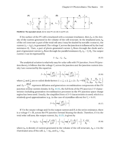
                 FIGURE 8.6  The equivalent circuit. (A) An ideal PV cell. (B) A real PV cell.

                   If the surface of the PV cell is irradiated with a constant irradiance, then J PV  is the den-
                 sity of the current generated in the volume of the cell structure. In the irradiated area A ill
                 of the cell structure (a part of the total cell area A may be shaded by metallic contacts), the
                 current I PV  = A ill J PV  is generated. The voltage V j  across the junction is influenced by the load
                 resistance R L . Then, a part of photo-generated current I d  flows through the diode and a
                 part of generated current I sh  flows through the parallel resistance R p , I sh  = V j /R p . The output
                 current I can be expressed by

                                                  I  = I PV  − I d  − I .                   (8.15)                                         I=IPV−Id−Ish.
                                                             sh
                   The analytical solution is relatively easy for solar cells with Pn junction. From Pn junc-
                 tion theory, it follows that the voltage V j  across the junction and the junction current den-
                 sity J are connected by the equation
                                                                    
                                       J  = J 01  exp   qV j    −  + J 02  exp  qV j    −  1 ,  (8.16)
                                                       1
                                                                 
                                                
                                                                   2
                                                ζ kT         ζ kT                                                                 J=J01expqVjζ 1 kT−1+J02expqVjζ 2
                                                  1
                                                                                     1       1  
                                                                                 D n    D p                                                         kT−1,
                                                                           = n q        +
                                                                              2
                 where ζ 1  and ζ 2  are so-called diode factors (1 ≤ ζ 1  ≤ 2, ζ 2  ≥ 2);  J 01  i                                       J01=ni2qDnLn1pp0+DpLp1nn0
                                                                                           p
                                                                                   n
                                                                                 Lp p0   Ln n0 
                          qn d
                        =   i   represent diffusion and generation-recombination components of the Pn
                 and  J 02                                                                                                                  J02=qnidτsc
                          τ sc
                 junction reverse current density. In eq. (8.16), the full form of the Pn junction I–V charac-
                 teristics including generation-recombination processes in the Pn junction space charge
                 region has been used. usually, the simplified form of I–V characteristics is used, which is a
                 relatively good approximation (e.g., in the case of crystalline silicon) for V j  > 0.4 V,
                                                               
                                                J  = J 01  exp  qV j    −  1 .          (8.17)
                                                        
                                                        ζ kT                                                                           J=J01expqVjζ 1 kT−1.
                                                          1
                   If V is the output voltage and I is the output current and R s  is the series resistance, there
                 is a voltage V + IR s  across the Pn junction forward biasing the diode. Therefore, if A is the
                 total solar cell area, the output current, eq. (8.15), is given by
                                            V  + R I         V  + R I     V  + R I
                             I  = A J  − I 01  exp  q  s    −  − I1  02  exp  q  s    −  −1  s  ,  (8.18)
                                 illPV
                                                                    2
                                                1
                                             ζ kT            ζ kT       R p                                                       I=AillJPV−I01expqV+RsIζ 1 kT−1−I
                                                                                                                                           02expqV+RsIζ 2 kT−1−V+RsIRp,
                 where J PV  is density of current generated in the volume of the cell structure, A ill  ≤ A is the
                 illuminated area of the cell, I 01  = AJ 01  and I 02  = AJ 02 .
   155   156   157   158   159   160   161   162   163   164   165