
Page 159 - A Comprehensive Guide to Solar Energy Systems
P. 159
160 A CoMPrehensIVe GuIde To soLAr enerGy sysTeMs
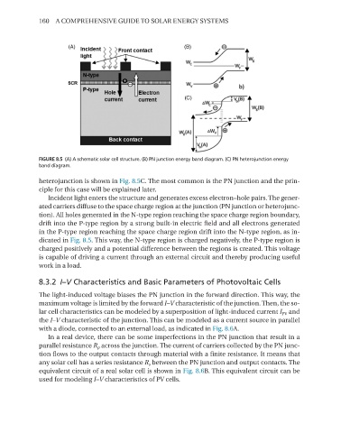
FIGURE 8.5 (A) A schematic solar cell structure. (B) PN junction energy band diagram. (C) PN heterojunction energy
band diagram.
heterojunction is shown in Fig. 8.5C. The most common is the Pn junction and the prin-
ciple for this case will be explained later.
Incident light enters the structure and generates excess electron–hole pairs. The gener-
ated carriers diffuse to the space charge region at the junction (Pn junction or heterojunc-
tion). All holes generated in the n-type region reaching the space charge region boundary,
drift into the P-type region by a strong built-in electric field and all electrons generated
in the P-type region reaching the space charge region drift into the n-type region, as in-
dicated in Fig. 8.5. This way, the n-type region is charged negatively, the P-type region is
charged positively and a potential difference between the regions is created. This voltage
is capable of driving a current through an external circuit and thereby producing useful
work in a load.
8.3.2 I–V Characteristics and Basic Parameters of Photovoltaic Cells
The light-induced voltage biases the Pn junction in the forward direction. This way, the
maximum voltage is limited by the forward I–V characteristic of the junction. Then, the so-
lar cell characteristics can be modeled by a superposition of light-induced current I PV and
the I–V characteristic of the junction. This can be modeled as a current source in parallel
with a diode, connected to an external load, as indicated in Fig. 8.6A.
In a real device, there can be some imperfections in the Pn junction that result in a
parallel resistance R p across the junction. The current of carriers collected by the Pn junc-
tion flows to the output contacts through material with a finite resistance. It means that
any solar cell has a series resistance R s between the Pn junction and output contacts. The
equivalent circuit of a real solar cell is shown in Fig. 8.6B. This equivalent circuit can be
used for modeling I–V characteristics of PV cells.