
Page 223 - A Comprehensive Guide to Solar Energy Systems
P. 223
226 A ComPRehenSIVe GuIDe To SolAR eneRGy SySTemS
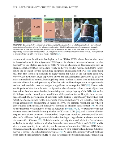
FIGURE 10.8 Scanning electron micrograph and schematic of the cross-section of a CdTe solar cell in the conventional
superstrate configuration (A) and the substrate configuration (B) which allows the use of opaque substrates such
as metal foils. In substrate configuration Mo/MoO x and i-ZnO/ZnO:Al are used as electrical back and front contact,
respectively. The scale bars correspond to 1 µm. The yellow arrows show the direction of illumination. (C) Photograph of
a sample with several CdTe solar cells on flexible metal foil [67].
structure of other thin film technologies such as CIGS or CZTS, where the absorber layer
is deposited prior to the n-type and TCo layers. An obvious question of course is, why
bother? The use of glass as a basis for CdTe PV modules has several disadvantages such as
it represents both 98% of the module weight and over a third of module cost. It also rather
limits the potential for use in building integrated photovoltaics (BIPV) [66], something
that thin film technologies should be highly suited for. CdTe in the substrate geometry,
where CdTe is the first layer deposited, allows for nontransparent substrates to be used
such as metal foils to be used. By using cheap metals such as stainless steel and aluminum
it would allow roll-to-roll processing of flexible cells and has the potential to significantly
reduce both module costs and weight, a significant advantage for BIPV [67]. From a sci-
entific point of view the substrate configuration also allows for a finer control of junction
formation, the chlorine activation, intermixing, and p-type doping of the CdTe [68] as the
CdTe layer can be treated prior to addition of the partner layers. Despite these advan-
tages though the performance of substrate CdTe devices is significantly lower than that
which has been achieved for the superstrate geometry, with only a few reports of over 10%
being achieved [69] and nothing in excess of 13.6%. The primary reason for the reduced
performance is the increased difficulty of forming an efficient back-contact [70]. As well
as the inherent work function issues discussed in Section 10.2.5, for substrate cells the
contact must also be self-forming, similar to CIGS and CZTS [71], and stable to all sub-
sequent deposition processes. The standard Cu process therefore becomes problematic
due to Cu diffusion during device fabrication leading to degradation and compensation
via excess Cu diffusion [72]. molybdenum is typically the metal of choice for substrate
cells due to its high purity and similar thermal expansion coefficient to CdTe [66] and is
also a known quantity to an extent given the volume of work in the CIGS and CZTS fields.
however, given the molybdenum work function of 4 eV a catastrophically large Schottky
barrier is present which hinders performance [70]. As a result the majority of work that has
been carried out on substrate CdTe PV thus far is focused on forming an ohmic contact via