
Page 219 - A Comprehensive Guide to Solar Energy Systems
P. 219
222 A ComPRehenSIVe GuIDe To SolAR eneRGy SySTemS
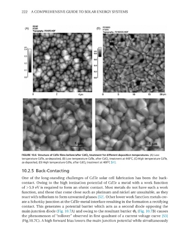
FIGURE 10.6 Structure of CdTe films before/after CdCl 2 treatment for different deposition temperatures. (A) Low
temperature CdTe, as-deposited, (B) Low temperature CdTe, after CdCl 2 treatment at 440°C, (C) High temperature CdTe,
as-deposited, (D) High temperature CdTe, after CdCl 2 treatment at 400°C [51].
10.2.5 Back-Contacting
one of the long-standing challenges of CdTe solar cell fabrication has been the back-
contact. owing to the high ionization potential of CdTe a metal with a work function
of >5.9 eV is required to form an ohmic contact. most metals do not have such a work
function, and those that come close such as platinum and nickel are unsuitable, as they
react with tellurium to form unwanted phases [52]. other lower work function metals cre-
ate a Schottky junction at the CdTe-metal interface resulting in the formation a rectifying
contact. This generates a potential barrier which acts as a second diode opposing the
main junction diode (Fig. 10.7A) and owing to the resultant barrier Φ b (Fig. 10.7B) causes
the phenomenon of “rollover” observed in first quadrant of a current voltage curve [53]
(Fig.10.7C). A high forward bias lowers the main junction potential while simultaneously