
Page 217 - A Comprehensive Guide to Solar Energy Systems
P. 217
220 A ComPRehenSIVe GuIDe To SolAR eneRGy SySTemS
with Si for example (which is typically >100 µm thick), but CdTe suffers from low carrier
lifetimes of typically <10 ns [34]. Indeed even determining the lifetime of CdTe to be this
large has proved problematic owing to particularly high surface recombination. Standard
time resolved photoluminescence measurements of the CdTe free surface give values dom-
inated by the surface recombination, leading to a large number of reports implying the car-
rier lifetime was <1 ns. This can be overcome to an extent by taking measurements through
the glass [35] but for a truly accurate analysis of the carrier lifetime a two-photon technique
is required [36], which gives a more accurate carrier lifetime value in the tens of nanosec-
ond range [34]. The low carrier lifetimes are in part due to the overriding issue with CdTe
thin films, the behavior of grain boundaries, which have been repeatedly linked to low per-
formance via issues such as low carrier lifetime [35]. It is widely believed these interstices
between the grains act as dominant recombination centers due to the presence of dangling
bonds. one of the recent primary challenges for CdTe solar cells has been understand the
role of the CdTe grain boundaries within functioning devices. The polycrystalline nature of
the films and the misorientation between neighboring grains, has been aptly demonstrated
by techniques such as electron back scattered diffraction [37], meaning one would indeed
anticipate a high defect density at the grain boundaries and for them to act as preferential
recombination centers. Although this thesis is supported by techniques such as cathodolu-
minescence, other techniques such as electron beam induced current (eBIC) have offered
contradictory evidence. For more information on the role of grain boundaries in CdTe solar
cells the reader is referred to the following review article on the subject [38]. Discussion
of the CdTe layer in isolation is problematic as the layer itself is never used in isolation.
All working devices require CdTe postgrowth treatments hence the discussion of the CdTe
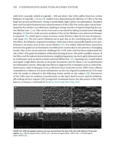
layer is, in essence, continued in Sections 10.2.4 and 10.2.5 Fig. 10.5.
FIGURE 10.5 SEM micrographs (surfaces and cross-sections) from the three CdTe films with different CSS growth
regimes. (A) +, (B) first regime (Tsub = 255°C), (C) +, (D) second regime (Tsub = 387°C), (E) +, (F) third regime
(Tsub = 523°C) [39].