
Page 214 - A Comprehensive Guide to Solar Energy Systems
P. 214
Chapter 10 • CdTe Solar Cells 217
10.2.1 Transparent Conductive Oxide (TCO)
For CdTe solar cells the choice of the TCo front-contact, requires careful consideration
because, unlike many other technologies, it employs the superstrate structure. Therefore,
as well as the usual TCo considerations of transparency and conductivity [5], as it is the
first layer deposited it also has the requirement to be stable to all subsequent deposition
processes. The processes that are to follow can therefore necessitate a particular choice of
TCo. Two of the more common TCos used for thin film PV are Sno 2 :In 2 o 3 (ITo) and Zno:Al
(AZo), both having low sheet resistance and high optical transparency. Both of these layers
can be problematic for CdTe cell fabrication though. AZo has a tendency to break down
at temperatures >400°C, losing conductivity, while ITo can similarly break down diffusing
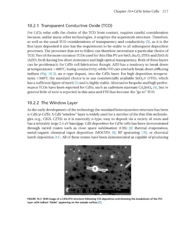
indium (Fig. 10.3), an n-type dopant, into the CdTe layer. For high deposition tempera-
tures >500°C the standard choice is to use commercially available Sno 2 :F (FTo), which
has a sufficient figure of merit [5] and is highly stable. Alternative bespoke and high perfor-
mance TCos have been reported for CdTe, such as cadmium stannate Cd 2 Sno 4 [6], but in
general little of note is reported in this area and FTo has become the “go to” TCo.
10.2.2 The Window Layer
As the early development of the technology the standard heterojunction structure has been
n-CdS/p-CdTe. A CdS “window” layer is widely used for a number of the thin film technolo-
gies (e.g., CIGS, CZTS) as it is nascently n-type, easy to deposit via a variety of routs and
has a tolerably large 2.4 eV bandgap. CdS deposition for CdTe cells has been demonstrated
through varied routes such as close space sublimation (CSS) [8] thermal evaporation,
metal-organic chemical vapor deposition (moCVD) [9], RF sputtering [10], or chemical
batch deposition [11]. All of these routes have been demonstrated as capable of producing
FIGURE 10.3 SEM image of a CdTe/ITO structure following CSS deposition and showing the breakdown of the ITO
layer with indium “blobs” appearing on the sample surface [7].