
Page 215 - A Comprehensive Guide to Solar Energy Systems
P. 215
218 A ComPRehenSIVe GuIDe To SolAR eneRGy SySTemS
device quality layers, but there are additional considerations that need to be factored in with
the CdS layer. Due to the superstrate nature of CdTe solar cells, the CdTe layer is deposited
on top of the CdS layer, often at higher temperatures than at which the CdS was deposited.
This leads to recrystallization of the CdS [12] and intermixing of the CdS and CdTe layers to
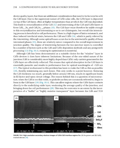
form CdS 1−x Te x and CdS y Te 1−y phases [13]. The CdS layer must therefore be stable enough
to this recrystallization and intermixing so as to not disintegrate, but overall this intermix-
ing process is beneficial to cell performance. There is a high degree of lattice mismatch, and
thus induced interfacial strain, between the CdS and CdTe [14], which is partly relieved by
the intermixing. Although some optical losses occur due to the semimetallic quality of these
intermixed phases [15], these are relatively minor compared to the overall improvement in
junction quality. The degree of intermixing between the two junction layers is controlled
by a number of factors such as the CdS and CdTe deposition methods and any postgrowth
processing [13] (Fig. 10.4), meaning its optimization is nontrivial.
Although CdS has been demonstrated as a suitable choice for the “window” layer in
CdTe devices it does have inherent limitations. Because of the one-sided nature of the
junction (CdS is considerably more highly doped than CdTe) only carriers generated in the
CdTe layer are effectively collected. This means that optical absorption in the CdS layer is
essentially parasitic and results in performance loss for optical wavelengths of <520 nm
[17]. The typical workaround to this problem has been to make the CdS as thin as possible
[18], thereby minimizing any such losses. This only works to a point however. Reducing
the CdS thickness too much, generally below around 100 nm, results in significant losses
in fill factor and open circuit voltage. The reason behind this is a question of microstruc-
ture, when the CdS is too thin voids, or pinholes as they are commonly referred to, begin to
form in the CdS layer [19] (Fig. 10.4). This can allow regions where the CdTe layer contacts
directly to the underlying oxide layer, weakening the average quality of the junction, and
bringing down the cell performance [20]. This may be overcome to an extent by the incor-
poration of a “buffer” or “highly resistive transparent” layer between the CdS and TCo
FIGURE 10.4 High-resolution secondary electron images of CdTe/CdS interface regions for. (A) As grown and (B) CdCl 2
treated devices [16].