
Page 220 - A Comprehensive Guide to Solar Energy Systems
P. 220
Chapter 10 • CdTe Solar Cells 223
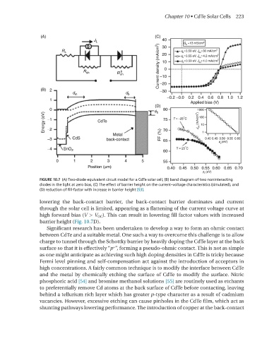
FIGURE 10.7 (A) Two-diode equivalent circuit model for a CdTe solar cell, (B) band diagram of two noninteracting
diodes in the light at zero bias, (C) The effect of barrier height on the current–voltage characteristics (simulated), and
(D) reduction of fill-factor with increase in barrier height [53].
lowering the back-contact barrier, the back-contact barrier dominates and current
through the solar cell is limited, appearing as a flattening of the current voltage curve at
high forward bias (V > V oC ). This can result in lowering fill factor values with increased
barrier height (Fig. 10.7D).
Significant research has been undertaken to develop a way to form an ohmic contact
between CdTe and a suitable metal. one such a way to overcome this challenge is to allow
charge to tunnel through the Schottky barrier by heavily doping the CdTe layer at the back
+
surface so that it is effectively “p ”, forming a pseudo-ohmic contact. This is not as simple
as one might anticipate as achieving such high doping densities in CdTe is tricky because
Fermi level pinning and self-compensation act against the introduction of acceptors in
high concentrations. A fairly common technique is to modify the interface between CdTe
and the metal by chemically etching the surface of CdTe to modify the surface. nitric
phosphoric acid [54] and bromine methanol solutions [55] are routinely used as etchants
to preferentially remove Cd atoms at the back surface of CdTe before contacting, leaving
behind a tellurium rich layer which has greater p-type character as a result of cadmium
vacancies. however, excessive etching can cause pinholes in the CdTe film, which act as
shunting pathways lowering performance. The introduction of copper at the back-contact