
Page 359 - A Comprehensive Guide to Solar Energy Systems
P. 359
364 A ComPRehensiVe Guide To soLAR eneRGy sysTems
Amorphous silicon cells have also been combined with nanocrystalline silicon junc-
tions [1] and the cells of other materials. Hetero-structures between a-Si:H layer and c-Si
wafer referred to as hiT (hetero-junction with intrinsic Thin film layer) cells have also
been developed and currently hold the record efficiency for crystalline Si. Panasonic man-
2
ufactured a cell of “practical size” (101 cm ) with an efficiency of 26.7% [7].
18.2.2 Cadmium Telluride Solar Cells
CdTe thin film solar cell structure comprises of a p-type CdTe absorber layer and n-type CdS
based window layer forming a heterojunction, which has an intermixed interface region. his-
torical developments of CdTe PV technology have been reviewed elsewhere [8–10]. CdTe thin
film absorbers possess good electronic property favorable for solar cells action. It has an ideal
direct band gap ∼1.5 eV which matches well with the maxima of the Sun’s spectrum offering
maximum theoretical efficiency ∼30% limit. The most attractive features of CdTe compound
are its chemical simplicity and the robust stability. CdTe is not only stable for terrestrial appli-
cations but it has also been demonstrated that CdTe has excellent stability under high ener-
gy-photon and electron irradiation for space applications, superior to si, GaAs, CiGs etc. [11].
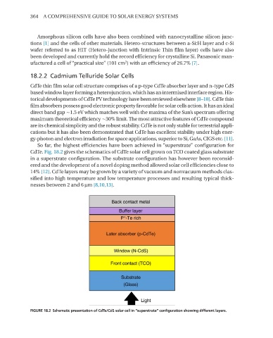
So far, the highest efficiencies have been achieved in “superstrate” configuration for
CdTe. Fig. 18.2 gives the schematics of CdTe solar cell grown on TCO coated glass substrate
in a superstrate configuration. The substrate configuration has however been reconsid-
ered and the development of a novel doping method allowed solar cell efficiencies close to
14% [12]. CdTe layers may be grown by a variety of vacuum and nonvacuum methods clas-
sified into high temperature and low temperature processes and resulting typical thick-
nesses between 2 and 6 µm [8,10,13].
FIGURE 18.2 Schematic presentation of CdTe/CdS solar cell in “superstrate” configuration showing different layers.