
Page 358 - A Comprehensive Guide to Solar Energy Systems
P. 358
Chapter 18 • Thin Film Photovoltaics 363
Compound thin film solar cells viz. CdTe, CiGs, mAPi etc. also provide advantage of
development of ternary, quaternary variants of the materials for the manipulation of the
band gap, which essentially can be used for development of tandem or multijunction solar
cells. This offers the possibility of significant absolute jump in efficiency with the cascade
of absorbers utilizing the wider part of the spectrum of light. The possibilities of develop-
ing CiGs/Perovskite or c-si/Perovskite is also being attempted by several groups, which
provides a theoretical efficiency limit over 40%, where practical efficiencies over 30% is
achievable with a marginal addition of processing costs.
18.2 Thin Film Cell Configurations
18.2.1 Amorphous Silicon
The intrinsic (i) form of a-si thin film can be doped as p-type or n-type to form a p-n junc-
tion, however, initial p-n junction device trials could not result in a solar cell action. This
was because of significant recombination losses due to the presence of a large number of
surface defects as dangling bonds in the material. The passivation of these defects are pos-
sible and hydrogen doped amorphous silicon, a-Si (H), could achieve significant efficien-
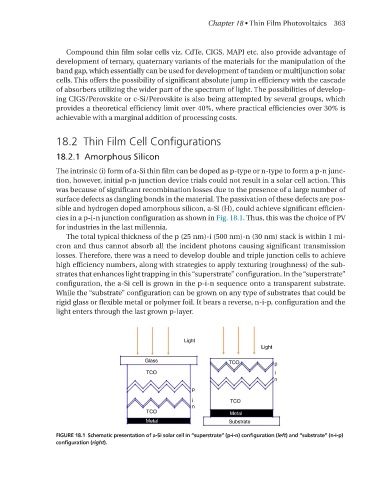
cies in a p-i-n junction configuration as shown in Fig. 18.1. Thus, this was the choice of PV
for industries in the last millennia.
The total typical thickness of the p (25 nm)-i (500 nm)-n (30 nm) stack is within 1 mi-
cron and thus cannot absorb all the incident photons causing significant transmission
losses. Therefore, there was a need to develop double and triple junction cells to achieve
high efficiency numbers, along with strategies to apply texturing (roughness) of the sub-
strates that enhances light trapping in this “superstrate” configuration. In the “superstrate”
configuration, the a-Si cell is grown in the p-i-n sequence onto a transparent substrate.
While the “substrate” configuration can be grown on any type of substrates that could be
rigid glass or flexible metal or polymer foil. It bears a reverse, n-i-p, configuration and the
light enters through the last grown p-layer.
FIGURE 18.1 Schematic presentation of a-Si solar cell in “superstrate” (p-i-n) configuration (left) and “substrate” (n-i-p)
configuration (right).