
Page 429 - A Comprehensive Guide to Solar Energy Systems
P. 429
Chapter 22 • Life Cycle Analysis of Photovoltaics: Strategic Technology Assessment 439
than we predicted, so we will present the EPBT and EROI results on an efficiency interval.
We have based our yield assumptions on the values reported in the ITRPV roadmap [12],
which are based on expert judgment. We address the yield uncertainty through parameter
uncertainty, as described in the previous subsection: industrial expert estimates receive a
data quality indicator score of 4 for reliability. Together with the other indicator scores one
can find the variance and 95% confidence interval of the yield assumptions, as outlined by
Weidema et al. [15]. Other sources of scenario uncertainty include development and adop-
tion of: diamond-coated wire sawing, encapsulation methods, double-sided contact cells,
and passivation methods. Finally, crystalline silicon PV modules might be produced by
processes in 2020 that are unknown today, or that we did not account for in our scenarios;
such uncertainties are discussed by mann et al. [9].
22.7 Results
22.7.1 Cells and Modules
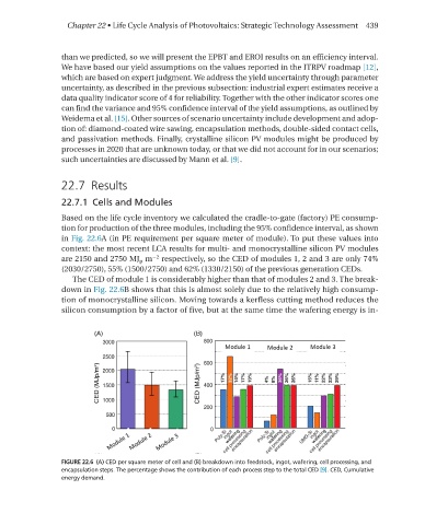
Based on the life cycle inventory we calculated the cradle-to-gate (factory) PE consump-
tion for production of the three modules, including the 95% confidence interval, as shown
in Fig. 22.6A (in PE requirement per square meter of module). To put these values into
context: the most recent LCA results for multi- and monocrystalline silicon PV modules
−2
are 2150 and 2750 mJ p m respectively, so the CEd of modules 1, 2 and 3 are only 74%
(2030/2750), 55% (1500/2750) and 62% (1330/2150) of the previous generation CEds.
The CEd of module 1 is considerably higher than that of modules 2 and 3. The break-
down in Fig. 22.6B shows that this is almost solely due to the relatively high consump-
tion of monocrystalline silicon. moving towards a kerfless cutting method reduces the
silicon consumption by a factor of five, but at the same time the wafering energy is in-
FIGURE 22.6 (A) CED per square meter of cell and (B) breakdown into feedstock, ingot, wafering, cell processing, and
encapsulation steps. The percentage shows the contribution of each process step to the total CED [9]. CED, Cumulative
energy demand.