
Page 425 - A Comprehensive Guide to Solar Energy Systems
P. 425
Chapter 22 • Life Cycle Analysis of Photovoltaics: Strategic Technology Assessment 435
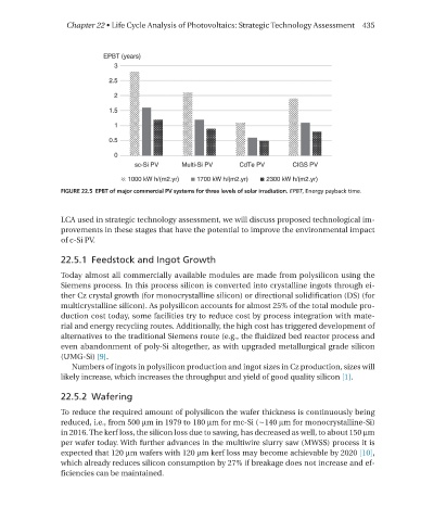
FIGURE 22.5 EPBT of major commercial PV systems for three levels of solar irradiation. EPBT, Energy payback time.
LCA used in strategic technology assessment, we will discuss proposed technological im-
provements in these stages that have the potential to improve the environmental impact
of c-Si PV.
22.5.1 Feedstock and Ingot Growth
Today almost all commercially available modules are made from polysilicon using the
Siemens process. In this process silicon is converted into crystalline ingots through ei-
ther Cz crystal growth (for monocrystalline silicon) or directional solidification (dS) (for
multicrystalline silicon). As polysilicon accounts for almost 25% of the total module pro-
duction cost today, some facilities try to reduce cost by process integration with mate-
rial and energy recycling routes. Additionally, the high cost has triggered development of
alternatives to the traditional Siemens route (e.g., the fluidized bed reactor process and
even abandonment of poly-Si altogether, as with upgraded metallurgical grade silicon
(umG-Si) [9].
numbers of ingots in polysilicon production and ingot sizes in Cz production, sizes will
likely increase, which increases the throughput and yield of good quality silicon [1].
22.5.2 Wafering
To reduce the required amount of polysilicon the wafer thickness is continuously being
reduced, i.e., from 500 µm in 1979 to 180 µm for mc-Si (∼140 µm for monocrystalline-Si)
in 2016. The kerf loss, the silicon loss due to sawing, has decreased as well, to about 150 µm
per wafer today. With further advances in the multiwire slurry saw (mWSS) process it is
expected that 120 µm wafers with 120 µm kerf loss may become achievable by 2020 [10],
which already reduces silicon consumption by 27% if breakage does not increase and ef-
ficiencies can be maintained.