
Page 330 - ARM Based Microcontroller Projects Using MBED
P. 330
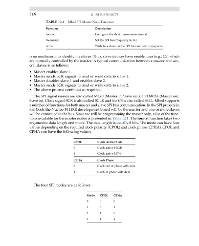
316                              12. SPI BUS PROJECTS

                          TABLE 12.1 Mbed SPI Master Node Functions
                          Function                   Description
                          format                     Configure the data transmission format
                          frequency                  Set the SPI bus frequency in Hz
                          write                      Write to a slave on the SPI bus and return response

                 is no mechanism to identify the slaves. Thus, slave devices have enable lines (e.g., CS) which
                 are normally controlled by the master. A typical communication between a master and sev-
                 eral slaves is as follows:
                 • Master enables slave 1.
                 • Master sends SCK signals to read or write data to slave 1.
                 • Master disables slave 1 and enables slave 2.
                 • Master sends SCK signals to read or write data to slave 2.
                 • The above process continues as required.
                   The SPI signal names are also called MISO (Master in, Slave out), and MOSI (Master out,
                 Slave in). Clock signal SCK is also called SCLK and the CS is also called SSEL. Mbed supports
                 a number of functions for both master and slave SPI bus communication. In the SPI projects in
                 this book the Nucleo-F411RE development board will be the master and one or more slaves
                 will be connected to the bus. Since we will be programming the master only, a list of the func-
                 tions available for the master nodes is presented in Table 12.1. The format function takes two
                 arguments: data length and mode. The data length is usually 8 bits. The mode can have four
                 values depending on the required clock polarity (CPOL) and clock phase (CPHA). CPOL and
                 CPHA can have the following values:


                                         CPOL         Clock Active State
                                         0            Clock active HIGH
                                         1            Clock active LOW
                                         CPHA         Clock Phase
                                         0            Clock out of phase with data
                                         1            Clock in phase with data


                   The four SPI modes are as follows:


                                                Mode   CPOL   CPHA
                                                0      0      0
                                                1      0      1
                                                2      1      0
                                                3      1      1