
Page 332 - ARM Based Microcontroller Projects Using MBED
P. 332
318 12. SPI BUS PROJECTS
12.3.2 Aim
The aim of this project is to show how an SPI bus compatible device can be connected to the
Nucleo-F411RE development board and also how it can be programmed using Mbed.
12.3.3 Block Diagram
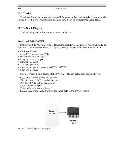
The block diagram of the project is shown in Fig. 12.2.
12.3.4 Circuit Diagram
In this project the MCP4921-type SPI bus compatible DAC chip is used. MCP4921 is a 12-bit
serial DAC manufactured by Microchip Inc., having the following basic specifications:
• 12-bit resolution
• up to 20MHz clock rate (SPI)
• fast settling time of 4.5μs
• unity or 2 gain output
• external V ref input
• 2.7–5.5V operation
• extended temperature range ( 40°C to +125°C)
• 8-pin DIL package
Fig. 12.3 shows the pin layout of the MCP4921. The pin definitions are as follows:
V DD ,AV SS : power supply and ground
CS: chip select (LOW to enable the chip)
SCK, SDI: SPI bus clock and data in
V OUTA : analog output
V REFA : reference input voltage
LDAC: DAC input latch (transfers the input data to the DAC registers.
FIG. 12.2 Block diagram of the project.