
Page 333 - ARM Based Microcontroller Projects Using MBED
P. 333
12.3 PROJECT 1—GENERATING SQUARE WAVE 319
V DD 1 8 V OUTA
CS 2 MCP4921 7 AV SS
SCK 3 6 V REFA
SDI 4 5 LDAC
FIG. 12.3 Pin layout of MCP4921 DAC.
Normally tied to ground so that CS controls the data transfer.
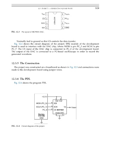
Fig. 12.4 shows the circuit diagram of the project. SPI2 module of the development
board is used to interface with the DAC chip, where MOSI is pin PC_3 and SCLK is pin
PC_7. The CS input of the DAC chip is connected to PC_0 of the development board.
The output of the DAC is connected to a PC-based oscilloscope in order to record the
generated waveform.
12.3.5 The Construction
The project was constructed on a breadboard as shown in Fig. 12.5 and connections were
made to the development board using jumper wires.
12.3.6 The PDL
Fig. 12.6 shows the program PDL.
FIG. 12.4 Circuit diagram of the project.