
Page 335 - ARM Based Microcontroller Projects Using MBED
P. 335
12.3 PROJECT 1—GENERATING SQUARE WAVE 321
12.3.7 The Program Listing
The digital input of a DAC converter can either be in serial or parallel form. In a parallel
converters the width of digital input is equal to the width of the converter. For example, a 12-
2
bit converter has 12 input bits. Serial converters in general use the SPI or the I C bus and ba-
sically a clock and a data signal are used to send data to the converter. Parallel converters
provide much faster conversion times but they are housed in larger packages. The DACs
are manufactured as either unipolar or bipolar as far as the output voltages are concerned.
Unipolar converters can provide only positive output voltages, whereas bipolar converters
provide both positive and negative voltages. In this book we will be using only unipolar
converters.
The relationship between the digital input-output and the voltage reference is given by
V o ¼DV ref /2 n
where V o is the output voltage, V ref the reference voltage, D the digital data, and n is the
width of the converter. For example, in a 12-bit converter (resolution¼12-bits) with +3.3V
reference voltage,
12
V o ¼3.3D/2 ¼0.805DmV
Thus, for example, if the input digital value is 1, the analog output voltage will be 0.805mV,
if the input value is 2, the analog output voltage will be 1.61mV, and so on.
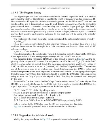
The program listing (program: SPIDAC) of the project is shown in Fig. 12.7. At the be-
ginning of the program SPI channel 2 is assigned to variable dac and PC_0 (CS of the DAC
chip) is configured as an output. Inside the main program, assuming a reference voltage of
3.3V, variable amplitude is set to 1V (1000mV) and the DAC chip is disabled. The remain-
der of the program runs in an endless loop. Inside this loop function DAC is called and
variable amplitude is sent as an argument to the function so that 1V analog signal is output
from the DAC. Then 0.5ms delay is inserted and 0 is sent to the DAC chip with again 0.5ms
delay so that the Duty Cycle of the signal is 50%. The loop is repeated until stopped
by the user.
Function DAC writes data to the DAC chip. Data is written to the DAC in two bytes. The
HIGH byte is sent first followed by the LOW byte. The lower byte specifies bits D0:D8 of the
digital input data. The upper byte consists of the following bits:
D8:D11: bits D8:D11 of the digital input data
SHDN: 1, output power down mode; 0, disable output buffer
GA: output gain control. 0, gain is 2 ; 1, gain is 1
BUF: 0, input unbuffered; 1, input buffered
A/B: 0, write to DAC A ; 1, write to DAC B (MCP4921 supports only DAC A )
Data is written to the DAC chip over the SPI bus using function dac.write.
Fig. 12.8 shows the generated output waveform on the oscilloscope.
12.3.8 Suggestions for Additional Work
Modify the program shown in Fig. 12.6 to generate a sawtooth waveform.