
Page 44 - Advances in Renewable Energies and Power Technologies
P. 44
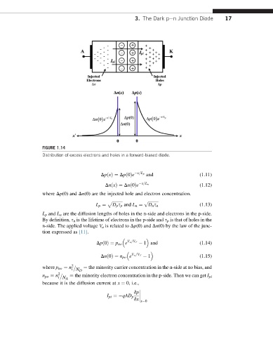
3. The Dark pen Junction Diode      17


                  FIGURE 1.14
                  Distribution of excess electrons and holes in a forward-biased diode.


                                         DpðxÞ¼ Dpð0Þe  x=L p  and              (1.11)
                                           DnðxÞ¼ Dnð0Þe  x=L n                 (1.12)
                  where Dp(0) and Dn(0) are the injected hole and electron concentration.
                                                          p
                                           p ffiffiffiffiffiffiffiffiffiffi     ffiffiffiffiffiffiffiffiffiffi
                                       L p ¼  D p s p and L n ¼  D n s n        (1.13)
                  L p and L n are the diffusion lengths of holes in the n-side and electrons in the p-side.
                  By definition, s n is the lifetime of electrons in the p-side and s p is that of holes in the
                  n-side. The applied voltage V a is related to Dp(0) and Dn(0) by the law of the junc-
                  tion expressed as [11].

                                       Dpð0Þ¼ p no e V a =V T    1 and          (1.14)

                                         Dnð0Þ¼ n po e V a =V T    1            (1.15)

                  where p no ¼ n 2    ¼ the minority carrier concentration in the n-side at no bias, and
                             i N D
                  n po ¼ n 2    ¼ the minority electron concentration in the p-side. Then we can get I pi
                        i N A
                  because it is the diffusion current at x ¼ 0, i.e.,

                                                      vp
                                           I pi ¼ qAD p
                                                      vx
                                                         x¼0