Page 43 - Advances in Renewable Energies and Power Technologies
P. 43
16     CHAPTER 1 Solar Cells and Arrays: Principles, Analysis, and Design


                         the metallurgical junction. They leave behind them un-neutralized acceptor and
                         donor ions as shown in Fig. 1.13. The electric field associated with the charges es-
                         tablishes opposing forces for further migration of holes and electrons, leading to
                         equilibrium such that no net current of either type exists. The width of this field re-
                         gion under no bias is of the order of few tenths of a micrometer depending on the
                         doping concentrations N A and N D . There is a potential difference associated with
                         this built-in or internal electric field. The name built-in comes from the fact that
                         this electric field is caused by the material inhomogeneity and not by an external
                         electric source. This built-in potential difference is termed the contact difference
                         of potential pointing out that such potential differences are formed if two dissimilar
                         materials are brought into intimate contact as in a pen junction where it could be
                         thought that a pen junction is formed by intimately contacting p- and n-type mate-
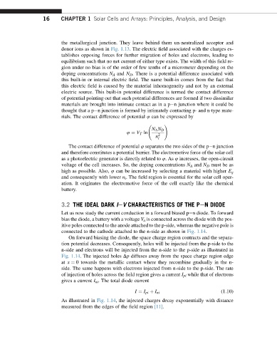
                         rials. The contact difference of potential 4 can be expressed by
                                                                 !
                                                            N A N D
                                                  4 ¼ V T ln   2
                                                              n
                                                               i
                            The contact difference of potential 4 separates the two sides of the pen junction
                         and therefore constitutes a potential barrier. The electromotive force of the solar cell
                         as a photoelectric generator is directly related to 4.As 4 increases, the open-circuit
                         voltage of the cell increases. So, the doping concentrations N A and N D must be as
                         high as possible. Also, 4 can be increased by selecting a material with higher E g
                         and consequently with lower n i . The field region is essential for the solar cell oper-
                         ation. It originates the electromotive force of the cell exactly like the chemical
                         battery.

                         3.2 THE IDEAL DARK IeV CHARACTERISTICS OF THE PeN DIODE
                         Let us now study the current conduction in a forward biased pen diode. To forward
                         bias the diode, a battery with a voltage V a is connected across the diode with the pos-
                         itive poles connected to the anode attached to the p-side, whereas the negative pole is
                         connected to the cathode attached to the n-side as shown in Fig. 1.14.
                            On forward biasing the diode, the space charge region contracts and the separa-
                         tion potential decreases. Consequently, holes will be injected from the p-side to the
                         n-side and electrons will be injected from the n-side to the p-side as illustrated in
                         Fig. 1.14. The injected holes Dp diffuses away from the space charge region edge
                         at x ¼ 0 towards the metallic contact where they recombine gradually in the n-
                         side. The same happens with electrons injected from n-side to the p-side. The rate
                         of injection of holes across the field region gives a current I pi while that of electrons
                         gives a current I ni . The total diode current

                                                      I ¼ I pi þ I ni                  (1.10)
                         As illustrated in Fig. 1.14, the injected charges decay exponentially with distance
                         measured from the edges of the field region [11].

