
Page 47 - Advances in Renewable Energies and Power Technologies
P. 47
20 CHAPTER 1 Solar Cells and Arrays: Principles, Analysis, and Design
2. Separate and collect the electrons and holes such that the electrons accumulate at
the negative pole while the holes accumulate at the positive pole. The separation
potential must be as high as possible.
The device that can perform these functions is the pen junction diode because its
semiconductor material absorbs photons and generates eeh pairs, and it has a sep-
aration potential in its transition region, which must be made as high as possible as
proved in the previous sections. So, a pen junction illuminated with the solar radi-
ation can produce electromotive force driving electric loads.
4.1 THE PV EFFECT OF A PeN SOLAR CELL
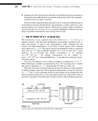
The construction, of a pen junction solar cell is shown in Fig. 1.16A.It isa pen
junction structure with full back metallization and partially metallized front to
allow the passage of light to the semiconductor while collecting the cell
current. The front metallization is in the form of metal fingers with a common
bus as shown in Fig. 1.16B. The typical construction parameters of the pen junction
þ
solar cell are [14]: The p-substrate thickness W p ¼ 0.20e0.5 mm, the n -layer
thickness W n ¼ 0.1e0.5 mm, the doping concentration of the substrate
16
3
þ
N A ¼ 10 e10 17 cm , the doping concentration of the emitter n -
18 19 3
layer ¼ 10 e10 /cm , the metal thickness ¼ 5 mm, and active material is mono-
crystalline silicon.
The solar cell behaves as a pen diode in darkness as indicated in Section 1.3.
When illuminated, it builds an electromotive force. We are going now to explain
this mode of operation. Fig. 1.17 illustrates the PV effect in a solar cell.
When the solar cell is irradiated with the sun light, the photons of light penetrate
to different depths where they will be absorbed and generate eeh pairs as shown in
Fig. 1.17.The eeh pairs generated within the field region will be separated by this
field such that the holes move to the p-side and the electrons to the n-side. Some of
the holes accumulate in the field region boundary of the p-side neutralizing part of it.
FIGURE 1.16
(A) The solar cell construction and (B) the front metallization.