
Page 42 - Advances in Renewable Energies and Power Technologies
P. 42
3. The Dark pen Junction Diode 15
Generally, the minimum semiconductor layer thickness to absorb light can be
expressed by
2
D min (1.9)
a
This simple relation is of a very critical importance for solar cell design. As the
semiconductors are expensive, one should use the minimum quantity of to perform
the absorption function. In this scenario, one needs thicker crystalline Si-layers as it
has the lowest a. This is true for thin-film solar cells. For wafer-based conventional
solar cells, the minimum layer thickness is limited by the mechanical rigidity.
3. THE DARK PeN JUNCTION DIODE
The commercial solar cells are basically pen junction diode structures constructed
to receive the solar radiation. To understand the operating principles underlying the
solar cell, one has to study first the pen junction diode. Solar cells are made of
either homotype pen junctions, heterotype junctions, or even multi-junction.
The homotype is from the same material, whereas the heterotype is from two
different materials. The operating principles are the same. So, we confine ourselves
to the homo junctions. The solar cell in darkness is a pen diode, whose dark char-
acteristics set the limits for the illuminated characteristics. From the principle
point of view, an illuminated solar cell ¼ a short circuit cell under light þ adark
biased pendiode.
3.1 FORMATION OF A FIELD REGION IN A PeN JUNCTION
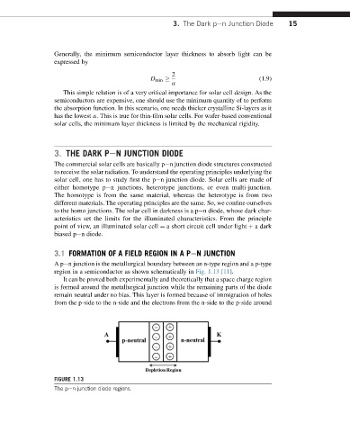
Apen junction is the metallurgical boundary between an n-type region and a p-type
region in a semiconductor as shown schematically in Fig. 1.13 [11].
It can be proved both experimentally and theoretically that a space charge region
is formed around the metallurgical junction while the remaining parts of the diode
remain neutral under no bias. This layer is formed because of immigration of holes
from the p-side to the n-side and the electrons from the n-side to the p-side around
FIGURE 1.13
The pen junction diode regions.