
Page 37 - Advances in Renewable Energies and Power Technologies
P. 37
10 CHAPTER 1 Solar Cells and Arrays: Principles, Analysis, and Design
FIGURE 1.6
The illustration of energy gap E g and energy level diagram.
2.2 DOPING AND CONDUCTIVITY OF THE MATERIAL
One of the main properties of the semiconductors is the possibility to alter their elec-
trical characteristics by doping. Doping is intentional addition of specific impurities
to the material to produce n-type or p-type conductors and change the electron and
hole concentration in the material. To produce n-type Si, we add pentavalent impu-
rity atoms to Si such as P and As, whereas for p-type Si, we add trivalent atoms such
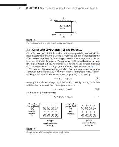
as B, Ga, and Al to Si. The charge picture after doping is illustrated in Fig. 1.7.
The product of the concentration p o and n o of any semiconductor at temperature
2
T are given by the relation n o p o ¼ n , which is called the mass action law. The con-
i
ductivity of the semiconductor material can be, generally, expressed by
(1.1)
s ¼ qm n o þ qm p o
n
p
where q is the electron charge; m n is the electron mobility; and m p is the hole
mobility. So, the conductivity of the n-type material is
s n z qm n o ¼ qm N D (1.2a)
n
n
and that of the p-type material is
s p z qm p o ¼ qm N A (1.2b)
p
p
FIGURE 1.7
Charge picture after doping the semiconductor silicon.