
Page 36 - Advances in Renewable Energies and Power Technologies
P. 36
2. Properties of Semiconductors for Solar Cells 9
2.1 THE ENERGY GAP E AND INTRINSIC CONCENTRATION N I
G
A semiconductor has an electron-filled valence band and an empty conduction band.
The two bands are separated by an energy gap E g . It ranges from few tenths of
electron-Volts to few electron-Volts. Silicon has an energy gap of 1.1 eV and
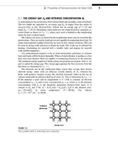
GaAs E g ¼ 1.45 eV. Elementary semiconductors are characterized by saturated co-
valent bonds as shown in Fig. 1.5, where each atom is bonded to the neighboring
atoms by four covalent bonds.
The valence electrons are shared by the neighboring atoms and are bound by the
parent atoms. They are locally fixed and are not capable of conducting electricity. To
make such materials conduct electricity we have to free valence electrons. This can
be done by doing work sufficient to break the bond. This work can be affected by
heating, illuminating the material with a suitable light, and doping the material
with suitable impurities.
Any semiconductor material works at room temperature, and hence, it contains
heat and bonds will be broken thermally. When a bond is broken, it produces a free
hole and a free electron. Both are capable of conducting electricity in the material.
The minimum energy required to break a bond and generate an electronehole (eeh)
pair is called the energy gap. The energy gap separates the free electrons from the
free holes as illustrated in Fig. 1.6.
The electrons are in the conduction band, where they occupy their lowest
allowed energy states with an effective overall density of N c ,whereas the
holes with positive charges occupy the allowed electronic states in the top of
valence band with an effective density of states N v . This is illustrated in Fig. 1.6.
If the material is pure and its temperature is T > 0 K, it contains an electron
concentration n o ¼ n i and a hole concentration p o ¼ n i ,where n i is the intrinsic
concentration with n i is the thermally generated electronehole pairs. It is
2
related to E g and T by n ¼ N c N v expð E g =k B TÞ. k B T is the thermal ener-
i
gy ¼ 25.6 meV at room temperature (T ¼ 300 K). For silicon,
10 3
n i ¼ 1.5 10 cm at 300 K.
FIGURE 1.5
The covalent bonds in elementary semiconductors.