
Page 35 - Advances in Renewable Energies and Power Technologies
P. 35
8 CHAPTER 1 Solar Cells and Arrays: Principles, Analysis, and Design
2. PROPERTIES OF SEMICONDUCTORS FOR SOLAR CELLS
In this section, the properties of semiconductors for solar cells will be introduced.
Solar cells are made of semiconductors as the active material. To understand the
operation of the solar cells and optimize their characteristics, one has to understand
thoroughly their material properties because there is a direct relationship between
the cell performance and the material properties.
Semiconductors are a class of materials that have electrical conductivity between
the metal and insulators. Accordingly, their electrical characteristics can be
controlled by doping and by light. They can be classified according to their chemical
structure in elementary form such as Si and Ge, in compound form such as A III B V
and A II B VI [7e9], or molecular form such as the organic semiconductors or the pe-
rovskites which are hybrid metal organic molecules [10]. All semiconductors have
common distinguished properties that govern their performance. The major proper-
ties controlling their electrical and optical behavior will be discussed in the next sub-
sections. The first property is the atomic structures of the materials. It has a large
impact on their performance. There are three distinct atomic arrangements for any
material:
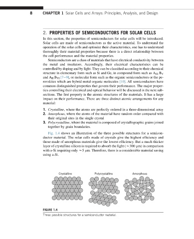
1. Crystalline, where the atoms are perfectly ordered in a three-dimensional array
2. Amorphous, where the atoms of the material have random order compared with
their original sites in the single crystal
3. Polycrystalline, where the material is composed of crystallographic grains joined
together by grain boundaries.
Fig. 1.4 shows an illustration of the three possible structures for a semicon-
ductor material. The solar cells made of crystals give the highest efficiency and
those made of amorphous materials give the lowest efficiency. But a much thicker
layer of crystalline silicon is required to absorb the light (w300 mm) in comparison
with a-Si requiring only w5 mm. Therefore, there is a considerable material saving
using a-Si.
Crystalline Polycrystalline Amorphous
FIGURE 1.4
Three possible structures for a semiconductor material.