
Page 80 - Advances in Renewable Energies and Power Technologies
P. 80
6. Circuit and Device Simulation of Solar Cells and Modules 53
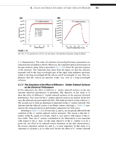
FIGURE 1.43
(A) The IeV characteristic of the npn structure, (B) spectral response using SILVACO.
IeV characteristics. The solar cell structure electrical performance parameters are
extracted and calculated as shown. Moreover, the simulated optical performance of
the npn structure using Atlas is presented. Fig. 1.43B shows the spectral response
of the structure. The important data taken from the figure are that the structure
responds well to the long-wavelength part of the input solar radiation spectrum,
which is the long-wavelength till the silicon cutoff wavelength 1.1 mm. This em-
phasizes that the vertical pn junction works very well as a long-wavelength
collector.
þ
6.2.4 The Simulation of the Effect of Different n Emitter Sidewall Surfaces
on the Electrical Performance
þ
In this subsection, the effect of different n emitter sidewall surfaces on the npn
structure electrical performance is presented. The objective of this study is to
þ
show the effect of different n emitter sidewall surfaces on the structure electrical
þ
performance. Two cases for the n emitter sidewall surfaces are studied. In the first
case, the sidewalls are passivated with SiO 2 . This indicates that it is done with low v s .
þ
The second case is when an aluminum is deposited on the n emitter sidewall. This
indicates that the sidewall surface is an Ohmic contact with high v s . Table 1.5 sum-
marizes the extracted electrical performance parameters for both cases.
Referring to Table 1.5, it is obvious that, I sc and J sc are not greatly affected by the
þ
condition of the n emitter sidewall surface treatment. The reason is that the n þ
emitter width W n equals to 0.18 mm, which is very narrow with respect to the p þ
base width. Thus, the n emitter contribution to the illumination is not important
þ
þ
with respect to the p base. As the main objective of the n emitter is to be a
þ
good one, the effect of its sidewall surface treatment on the dark characteristics,
the reverse saturation current (I o ) and V oc , is more important. In this study, it is
þ
important to calculate I s as its value well clarifies the effect of n emitter sidewall