
Page 79 - Advances in Renewable Energies and Power Technologies
P. 79
52 CHAPTER 1 Solar Cells and Arrays: Principles, Analysis, and Design
Then the starting material is invoked along with its doping. This process is fol-
lowed by etching Si wafer to deposit the oxide.
init silicon c.boron¼1.0e18 orientation ¼ 111
ETCH silicon START X ¼ 8Y ¼ 0.0
ETCH CONTINUE X ¼ 8.5 Y ¼ 0.0
ETCH CONTINUE X ¼ 8.5 Y ¼ 75
ETCH DONE X ¼ 8Y ¼ 75
Deposit oxide thickness ¼ 0.1 div ¼ 2
etch oxide right p1.x ¼ 8
After that, diffusion of the emitter is performed.
Diffuse time ¼ 2 temp ¼ 1000 phosphorus ¼ 2e20
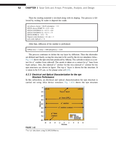
The process continues to define the top layer by diffusion. Then the electrodes
are defined and finally saving the structure to be used by the device simulator Atlas.-
Fig. 1.42 shows the npn structure produced by Athena. The cathode is taken as a con-
þ
þ
tact for n emitter from sidewall. The anode is taken as a contact for p base from
þ
þ
back surface. Also, the sidewall n emitter for the two-sidewall n emitter for the
þ
npn structures are shown in figure. The top n layer is shown for the structure. It
is taken to be 0.25 mm, as for planar solar cell [48].
6.2.3 Electrical and Optical Characterization for the npn
Structure Performance
In this subsection, an electrical and optical characterization the npn structure is
carried out using Atlas device simulator. Fig. 1.43A shows the npn structure
FIGURE 1.42
The npn structure using SILVACO/Athena.