
Page 77 - Advances in Renewable Energies and Power Technologies
P. 77
50 CHAPTER 1 Solar Cells and Arrays: Principles, Analysis, and Design
(A) (B)
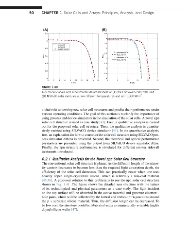
FIGURE 1.40
IeV model curves and experimental data/datasheet of (A) the Photowatt-PWP 201 and
2
(B) MSX-60 solar modules at two different temperatures and G ¼ 1000 W/m .
a vital role to develop new solar cell structures and predict their performance under
various operating conditions. The goal of this section is to clarify the importance of
using process and device simulators in the simulation of the solar cells. A novel npn
solar cell structure is used as case study [43]. First, a qualitative analysis is carried
out for the proposed solar cell structure. Then, the qualitative analysis is quantita-
tively verified using SILVACO device simulator [44]. In the quantitative analysis,
first, an explanation for how to construct the solar cell structure using SILVACO pro-
cess simulator Athena is presented. Second, the electrical and optical performance
parameters are presented using the output from SILVACO device simulator Atlas.
Finally, the npn structure performance is simulated for different emitter sidewall
treatments introduced.
6.2.1 Qualitative Analysis for the Novel npn Solar Cell Structure
The conventional solar cell structure is planar. As the diffusion length of the minor-
ity carriers decreases to become less than the required light absorption depth, the
efficiency of the solar cell decreases. This can practically occur when one uses
heavily doped single-crystalline silicon, which is relatively a low-cost material
[45,46]. A proposed solution to this problem is to use the npn solar cell structure
shown in Fig. 1.41. The figure shows the detailed npn structure with the values
of its technological and physical parameters as a case study. The light incident
on the top surface will be absorbed in the active material and generate electrone
hole pairs, which will be collected by the lateral and vertical pen junctions around
the p þ substrate silicon material. Thus, the diffusion length can be decreased. To
be low cost, the structure could be fabricated using a commercially available highly
doped silicon wafer [47].