
Page 78 - Advances in Renewable Energies and Power Technologies
P. 78
6. Circuit and Device Simulation of Solar Cells and Modules 51
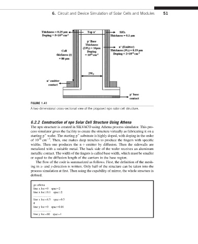
FIGURE 1.41
A two-dimensional cross-sectional view of the proposed npn solar cell structure.
6.2.2 Construction of npn Solar Cell Structure Using Athena
The npn structure is created in SILVACO using Athena process simulator. This pro-
cess simulator gives the facility to create the structure virtually as fabricating it on a
þ
þ
starting p wafer. The starting p substrate is highly doped, with doping in the order
3
of 10 18 cm . Then, one makes deep trenches to produce the fingers with specific
widths. Then one produces the n þ emitter by diffusion. Then the sidewalls are
metalized with a suitable metal. The back side of the wafer receives an aluminum
metallic contact. The width of the fingers is called base width, which must be smaller
or equal to the diffusion length of the carriers in the base region.
The flow of the code is summarized as follows. First, the definition of the mesh-
ing in x- and y-direction is written. Only half of the structure can be taken into the
process simulation at first. Then using the capability of mirror, the whole structure is
defined.
go athena
line x loc¼0 spac¼2
line x loc¼0.1 spac¼2
......
line x loc¼8.5 spac¼0.5
#
line y loc¼0 spac¼0.01
......
line y loc¼80 spac¼1