
Page 107 - An Introduction to Microelectromechanical Systems Engineering
P. 107
86 MEM Structures and Systems in Industrial and Automotive Applications
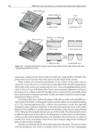
Silicon frame
{111}
Silicon nitride {111}
Silicon
1. Pattern mask 2. Anisotropic etch
Resist p++ silicon
Silicon frame
p++
silicon
Silicon
1. Pattern mask 2. Etch circle in p++
Silicon
nitride
3. Mask front side 4. Anisotropic etch
Figure 4.3 Schematic illustrations of square and circular nozzles on the wafer surface with their
corresponding fabrication steps.
anisotropic etching of the silicon from the back side using KOH or TMAH. The
p-type layer acts as an etch stop, thus preserving the shape of the nozzle.
These nozzles are oriented perpendicular to the surface of the wafer and are
referred to as top shooters or roof shooters in the inkjet field. Nozzles oriented par-
allel to the wafer surface are termed side shooters. One such implementation devel-
oped by Xerox Corp. of Webster, New York, uses orientation-dependent etching to
form grooves in a silicon wafer [8]. Another wafer is coated with a polyimide spacer
layer and bonded to the grooved wafer. Finally, the wafer is diced to reveal triangle-
shaped ports [Figure 4.4(a)].
Choosing a fluid flow path in the plane of the silicon wafer and using RIE pro-
vides further flexibility in shaping the nozzle and the orifices. In an implementation
ofaCO cleaning apparatus [9], a silicon micromachined nozzle was specially
2
designed to allow subsonic fluid flow at the inlet and supersonic flow at the outlet
[Figure 4.4(b)]. DRIE is a suitable process for defining in the silicon a deep channel
(50 to 500 µm) following the desired contour of the nozzle. The dimensional control
is limited in the plane of the wafer by the lithography to better than one micrometer,
whereas in the vertical depth direction, it is limited by the etch process to approxi-
mately 10% of the total depth. A top cover is later bonded using anodic bonding of
glass or silicon fusion bonding.
Nozzles can alternatively be fabricated using electroforming. The process starts
with the production of a mold or mandrel, which may be flat or have topography