
Page 179 - An Introduction to Microelectromechanical Systems Engineering
P. 179
158 MEM Structures and Systems in Photonic Applications
of delivering such high angular pointing precision, as well complex alignment and
closed-loop feedback systems that are beyond the scope of this book [35].
Many companies achieved significant progress in the development of
very-large-scale photonic switches (reaching up to 4,000 × 4,000). However the col-
lapse of the telecommunications capital equipment market by 2002 forced many of
these companies to use their micromirror technologies in pursuit of other, possibly
less lucrative, markets. It is the broad utility of these beam-steering micromirrors
that leads us to present them here, even though the primary application for which
they were developed (fiber-optical telecommunication) will not witness significant
growth until a future time.
A search on issued patents in this field reveals a plurality of micromirror
inventions, the vast majority of which utilize electrostatic actuation (e.g., [36]).
One implementation from Integrated Micromachines, Inc. (IMMI), of Irwindale,
California, utilizes electromagnetic actuation instead. While the company is no
longer pursuing applications in fiber-optical communications, the design stands out
as an elegant implementation using a low-voltage, low-power electromagnetic
scheme [37].
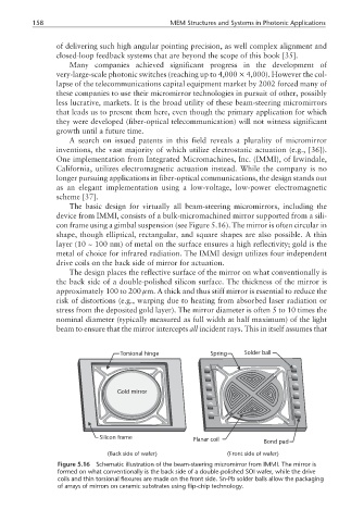
The basic design for virtually all beam-steering micromirrors, including the
device from IMMI, consists of a bulk-micromachined mirror supported from a sili-
con frame using a gimbal suspension (see Figure 5.16). The mirror is often circular in
shape, though elliptical, rectangular, and square shapes are also possible. A thin
layer (10 ~ 100 nm) of metal on the surface ensures a high reflectivity; gold is the
metal of choice for infrared radiation. The IMMI design utilizes four independent
drive coils on the back side of mirror for actuation.
The design places the reflective surface of the mirror on what conventionally is
the back side of a double-polished silicon surface. The thickness of the mirror is
approximately 100 to 200 µm. A thick and thus stiff mirror is essential to reduce the
risk of distortions (e.g., warping due to heating from absorbed laser radiation or
stress from the deposited gold layer). The mirror diameter is often 5 to 10 times the
nominal diameter (typically measured as full width at half maximum) of the light
beam to ensure that the mirror intercepts all incident rays. This in itself assumes that
Torsional hinge Spring Solder ball
Gold mirror
Silicon frame Planar coil Bond pad
(Back side of wafer) (Front side of wafer)
Figure 5.16 Schematic illustration of the beam-steering micromirror from IMMI. The mirror is
formed on what conventionally is the back side of a double-polished SOI wafer, while the drive
coils and thin torsional flexures are made on the front side. Sn-Pb solder balls allow the packaging
of arrays of mirrors on ceramic substrates using flip-chip technology.