
Page 233 - An Introduction to Microelectromechanical Systems Engineering
P. 233
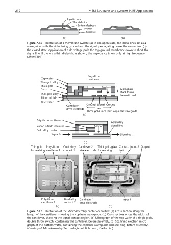
212                                        MEM Structures and Systems in RF Applications

                                        Top electrode
                                            Thin dielectric
                                               Bottom electrode
                                                  Isolation
                                                    Substrate

                                      (a)                               (b)
                 Figure 7.16  Illustration of a membrane switch: (a) In the open state, the metal lines act as a
                 waveguide, with the sides being ground and the signal propagating down the center line. (b) In
                 the closed state, application of a dc voltage pulls the top ground membrane down to short the
                 signal line. If there is a thin dielectric as shown, the impedance is low only at high frequency.
                 (After: [30].)


                                                     Polysilicon
                         Cap wafer                   cantilever
                         Thin gold alloy
                         Thick gold                          Motion
                         Glass                                          Gold/glass
                                                                        stack forms
                         Thin gold alloy
                                                                        hermetic seal
                         Silicon nitride
                         Base wafer
                                        Cantilever  Ground  Signal  Ground
                                        drive electrode
                                                    Three gold lines form coplanar waveguide
                                                  (a)
                       Polysilicon cantilever
                                                                  Gold alloy
                       Silicon nitride insulator        Motion    signal line
                       Gold alloy contact
                               Signal in                                Signal out

                                                  (b)
                   Thin gold  Polysilicon  Gold alloy  Cantilever 2  Thick gold/glass Contact  Input 2 Output
                   for seal ring cantilever 1  contact 1  drive electrode  for seal ring  area


                         Polysilicon   Gold alloy  Cantilever 1          Input 1
                         cantilever 2  contact 2  drive electrode
                                  (c)                            (d)
                 Figure 7.17  Illustration of the MicroAssembly cantilever switch: (a) Cross section along the
                 length of the cantilever, showing the coplanar waveguide. (b) Cross section across the width of
                 the cantilever, showing the signal contact region. (c) Micrograph of the top wafer of a single-pole,
                 double-throw switch, containing the cantilever, before assembly. (d) Scanning electron micro-
                 graph of the bottom wafer, containing the coplanar waveguide and seal ring, before assembly.
                 (Courtesy of: MicroAssembly Technologies of Richmond, California.)