
Page 231 - An Introduction to Microelectromechanical Systems Engineering
P. 231
210 MEM Structures and Systems in RF Applications
to date, pairs of FBAR filters have been placed at the antenna of a cellular phone to
form a duplexer. One bandpass filter allows signal transmission from the output
power amplifier to the antenna (e.g., 1.85–1.91 GHz for PCS); the other has a differ-
ent bandpass that transmits received signals from the antenna to the input low-noise
amplifier (e.g., 1.93–1.99 GHz for PCS).
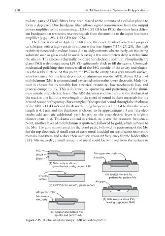
The fabrication of an Agilent FBAR filter, the exact details of which are proprie-
tary, begins with a high-resistivity silicon wafer (see Figure 7.15) [27, 28]. The high
resistivity is needed to reduce losses due to eddy currents; alternatively, an insulating
substrate such as glass could be used. A cavity a few micrometers deep is etched into
the silicon. The silicon is thermally oxidized for electrical isolation. Phosphosilicate
glass (PSG) is deposited using LPCVD sufficiently thick to fill the cavity. Chemical-
mechanical polishing then removes all of the PSG outside of the cavity and planar-
izes the wafer surface. At this point, the PSG in the cavity has a very smooth surface,
which is critical for the later deposition of aluminum nitride (AlN). About 0.1 µmof
molybdenum (Mo) is sputtered and patterned to form the lower electrode. Molybde-
num is chosen for its suitably low electrical resistivity, low mechanical loss, and
process compatibility. This is followed by sputtering and patterning of the alumi-
num nitride piezoelectric layer. The AlN thickness is chosen so that the thickness of
the stack is one half of a wavelength of the speed of sound in these materials for the
desired resonant frequency. For example, if the speed of sound through the thickness
of the AlN is 11.4 km/s and the desired tuning frequency is 1.88 GHz, then the wave-
length is 6.1 µm and the thickness is chosen to be approximately 3 µm (the elec-
trodes add acoustic additional path length, so the piezoelectric layer is slightly
thinner than this). Thickness control is critical, as it sets the resonant frequency.
Next, another layer of molybdenum is sputtered, followed by gold, which adheres to
the Mo. The gold is patterned for the bond pads, followed by patterning of the Mo
for the top electrode. A small area of extra metal is added on top of some resonators
to mass-load them and reduce their acoustic resonant frequency for the ladder filter
[28]. Alternatively, a small amount of metal could be removed from the surface to
PSG
Mo upper electrode
Oxide
Au pad
Silicon
(1) Etch cavity in silicon,
grow thermal oxide, deposit PSG
(4) Sputter Mo and Au,
Smooth pattern Au, pattern Mo
surface
Air gap
(2) CMP PSG for smooth, planar surface
AlN piezoelectric
Mo lower
electrode (5) Etch away sacrifical PSG,
leaving suspended FBAR
(3) Sputter and pattern Mo,
sputter and pattern AlN
Figure 7.15 Illustration of an example FBAR fabrication process.