
Page 234 - An Introduction to Microelectromechanical Systems Engineering
P. 234
Microelectromechanical Switches 213
Membrane Shunt Switch
In a membrane-switch implementation from the University of Michigan, Ann
Arbor, Michigan, a 2-µm-thick layer of gold is suspended 2 µm above a
0.8-µm-thick gold signal line, which is coated with about 0.15 µm of insulating sili-
con nitride [30]. The membranes have a span of 300 µm and lengths of 20 to 140
µm. Application of a 15-V dc voltage to the signal line (in addition to the ac signal)
pulls the gold membrane down to the nitride, shunting the signal line to ground
[31]. The use of an insulator prevents this switch from working at dc and low fre-
quency but is expected to be more reliable than metal-to-metal contacts. The sides
of the gold membrane are supported by wide strips of the same gold film,
which, with the signal line, form the coplanar waveguide needed for microwave
signals.
In the closed state, the connection is made by capacitive coupling, which is only
useful at high frequency. Insertion loss in the closed state is less than 0.6 dB over the
range of 10–40 GHz, with a return loss of less than –20 dB. The silicon nitride could
be made even thinner for a lower closed-state capacitance and lower insertion loss,
but it is already at the minimum thickness required to prevent breakdown with the
required dc operation voltage. In the open state, there is clearly a capacitor that
causes undesired coupling. The gap could be increased for greater isolation (at least
20 dB is desired), but this would require an even greater actuation voltage. The
measured ratio of closed to open capacitance in this design is about 17. The loss in
the up state is the same as for the coplanar waveguide alone.
Cantilever Series Switch
Several cantilever-type switches with metal-to-metal contacts (also known as relays)
are under commercial development by companies such as Teravicta Technologies of
Austin, Texas; Radant MEMS, Inc., of Stowe, Massachusetts; and MicroAssembly
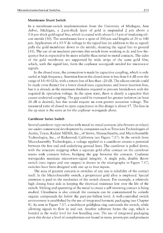
Technologies, Inc., of Richmond, California (see Figure 7.17). In the switch from
MicroAssembly Technologies, a voltage applied to a cantilever creates a potential
between the free end and underlying ground lines. The cantilever is pulled down,
with the structure stopping when a separate gold-alloy contact on the cantilever
mates with contacts below, bridging the gap between the contacts. Coplanar
waveguides maintain microwave-signal integrity. A single pole, double throw
switch (two inputs and one output) is shown in the micrographs in Figure 7.17;
switches have been designed with one up to four inputs.
The area of greatest concern in switches of any size is reliability of the contact
itself. In the MicroAssembly switch, a proprietary gold alloy is employed. Special
attention is paid to the mechanics of the switch closure. For example, a relatively
high closing force aids in keeping the electrical resistance low over the life of the
switch. Melting and sputtering of the metal to create a self-renewing contact is being
studied. Cleanliness is also critical: the contacts can be contaminated by volatile
organic compounds far below the part-per-billion level. A well-controlled switch
environment is established by the use of integrated hermetic packaging (see Chapter
8). As seen in Figure 7.17, a multilayer gold/glass ring surrounds the switch, while
allowing signals to flow in and out. Another substrate forms the cap, which is
bonded at the wafer level for low handling cost. The use of integrated packaging
gives this device a level of completeness not found in many prototypes and produces