
Page 239 - An Introduction to Microelectromechanical Systems Engineering
P. 239
218 Packaging and Reliability Considerations for MEMS
technologies will penetrate MEMS remains to be seen, but if they do they will cer-
tainly have to rely on serious market incentives, in particular high-volume applica-
tions, and on a minimum level of technology standardization.
The field of packaging is so broad in scope that one can only hope to present
here a brief introduction of the fundamentals (see Figure 8.1), especially as they
relate to the various structures and systems introduced in the previous chapters.
Such an accomplishment is made more difficult by the proprietary nature of most
package designs.
Key Design and Packaging Considerations
Designing packages for micromachined sensors and actuators involves taking into
account a number of important factors. Some are shared with the packaging of elec-
tronic integrated circuits, but many are specific to the application. These factors also
bear significance on the design of the micromachined components themselves. As a
result, the design of the package and of the micromachined structures must com-
mence and evolve together; it would be naïve to believe they can be separated. The
following are critical factors and considerations frequently encountered in MEMS
packaging.
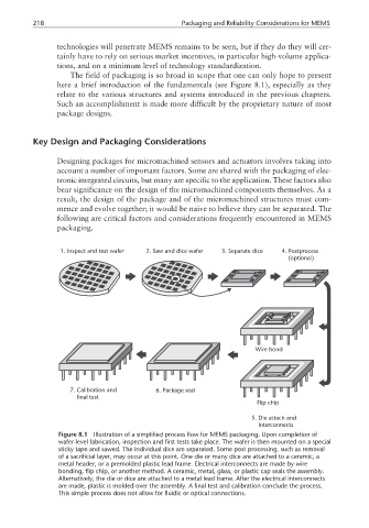
1. Inspect and test wafer 2. Saw and dice wafer 3. Separate dice 4. Postprocess
(optional)
Wire bond
7. Calibration and 6. Package seal
final test
Flip chip
5. Die attach and
interconnects
Figure 8.1 Illustration of a simplified process flow for MEMS packaging. Upon completion of
wafer-level fabrication, inspection and first tests take place. The wafer is then mounted on a special
sticky tape and sawed. The individual dice are separated. Some post processing, such as removal
of a sacrificial layer, may occur at this point. One die or many dice are attached to a ceramic, a
metal header, or a premolded plastic lead frame. Electrical interconnects are made by wire
bonding, flip chip, or another method. A ceramic, metal, glass, or plastic cap seals the assembly.
Alternatively, the die or dice are attached to a metal lead frame. After the electrical interconnects
are made, plastic is molded over the assembly. A final test and calibration conclude the process.
This simple process does not allow for fluidic or optical connections.