
Page 62 - An Introduction to Microelectromechanical Systems Engineering
P. 62
Basic Process Tools 41
The mask itself consists of a patterned opaque chromium (the most common),
emulsion, or iron oxide layer on a transparent fused-quartz or soda-lime glass sub-
strate. The pattern layout is generated using a computer-aided design (CAD) tool
and transferred into the opaque layer at a specialized mask-making facility, often by
electron-beam or laser-beam writing. A complete microfabrication process nor-
mally involves several lithographic operations with different masks.
Positive photoresist is an organic resin material containing a sensitizer. It is
spin-coated on the wafer with a typical thickness between 0.5 µm and 10 µm. As
mentioned earlier, special types of resists can be spun to thicknesses of over 200
µm, but the large thickness poses significant challenges to exposing and defining
features below 25 µm in size. The sensitizer prevents the dissolution of unexposed
resist during immersion in the developer solution. Exposure to light in the 200- to
450-nm range (ultraviolet to blue) breaks down the sensitizer, causing exposed
regions to immediately dissolve in developer solution. The exact opposite process
happens in negative resists—exposed areas remain and unexposed areas dissolve in
the developer.
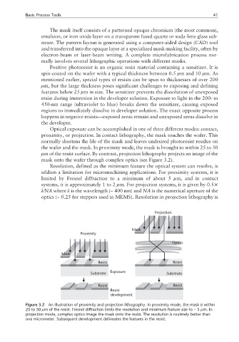
Optical exposure can be accomplished in one of three different modes: contact,
proximity, or projection. In contact lithography, the mask touches the wafer. This
normally shortens the life of the mask and leaves undesired photoresist residue on
the wafer and the mask. In proximity mode, the mask is brought to within 25 to 50
µm of the resist surface. By contrast, projection lithography projects an image of the
mask onto the wafer through complex optics (see Figure 3.2).
Resolution, defined as the minimum feature the optical system can resolve, is
seldom a limitation for micromachining applications. For proximity systems, it is
limited by Fresnel diffraction to a minimum of about 5 µm, and in contact
systems, it is approximately 1 to 2 µm. For projection systems, it is given by 0.5×
λ⁄NA where λ is the wavelength (~ 400 nm) and NA is the numerical aperture of the
optics (~ 0.25 for steppers used in MEMS). Resolution in projection lithography is
Projection
Mask
Proximity
Optics
Mask
Resist Resist
Substrate Exposure Substrate
Resist Resist
Resist
development
Figure 3.2 An illustration of proximity and projection lithography. In proximity mode, the mask is within
25 to 50 µm of the resist. Fresnel diffraction limits the resolution and minimum feature size to ~ 5 µm. In
projection mode, complex optics image the mask onto the resist. The resolution is routinely better than
one micrometer. Subsequent development delineates the features in the resist.