
Page 65 - An Introduction to Microelectromechanical Systems Engineering
P. 65
44 Processes for Micromachining
Mask alignment keys Front side Microscope view
Mask
Wafer
Chuck
Wafer alignment keys
Microscope
(a) objectives
(b)
Y
X
(c)
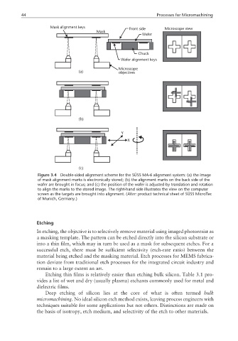
Figure 3.4 Double-sided alignment scheme for the SÜSS MA-6 alignment system: (a) the image
of mask alignment marks is electronically stored; (b) the alignment marks on the back side of the
wafer are brought in focus; and (c) the position of the wafer is adjusted by translation and rotation
to align the marks to the stored image. The right-hand side illustrates the view on the computer
screen as the targets are brought into alignment. (After: product technical sheet of SÜSS MicroTec
of Munich, Germany.)
Etching
In etching, the objective is to selectively remove material using imaged photoresist as
a masking template. The pattern can be etched directly into the silicon substrate or
into a thin film, which may in turn be used as a mask for subsequent etches. For a
successful etch, there must be sufficient selectivity (etch-rate ratio) between the
material being etched and the masking material. Etch processes for MEMS fabrica-
tion deviate from traditional etch processes for the integrated circuit industry and
remain to a large extent an art.
Etching thin films is relatively easier than etching bulk silicon. Table 3.1 pro-
vides a list of wet and dry (usually plasma) etchants commonly used for metal and
dielectric films.
Deep etching of silicon lies at the core of what is often termed bulk
micromachining. No ideal silicon etch method exists, leaving process engineers with
techniques suitable for some applications but not others. Distinctions are made on
the basis of isotropy, etch medium, and selectivity of the etch to other materials.