
Page 64 - An Introduction to Microelectromechanical Systems Engineering
P. 64
Basic Process Tools 43
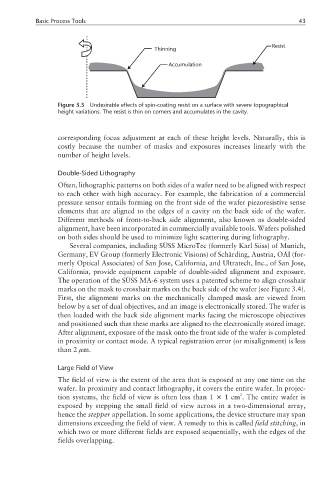
Resist
Thinning
Accumulation
Figure 3.3 Undesirable effects of spin-coating resist on a surface with severe topographical
height variations. The resist is thin on corners and accumulates in the cavity.
corresponding focus adjustment at each of these height levels. Naturally, this is
costly because the number of masks and exposures increases linearly with the
number of height levels.
Double-Sided Lithography
Often, lithographic patterns on both sides of a wafer need to be aligned with respect
to each other with high accuracy. For example, the fabrication of a commercial
pressure sensor entails forming on the front side of the wafer piezoresistive sense
elements that are aligned to the edges of a cavity on the back side of the wafer.
Different methods of front-to-back side alignment, also known as double-sided
alignment, have been incorporated in commercially available tools. Wafers polished
on both sides should be used to minimize light scattering during lithography.
Several companies, including SÜSS MicroTec (formerly Karl Süss) of Munich,
Germany, EV Group (formerly Electronic Visions) of Schärding, Austria, OAI (for-
merly Optical Associates) of San Jose, California, and Ultratech, Inc., of San Jose,
California, provide equipment capable of double-sided alignment and exposure.
The operation of the SÜSS MA-6 system uses a patented scheme to align crosshair
marks on the mask to crosshair marks on the back side of the wafer (see Figure 3.4).
First, the alignment marks on the mechanically clamped mask are viewed from
below by a set of dual objectives, and an image is electronically stored. The wafer is
then loaded with the back side alignment marks facing the microscope objectives
and positioned such that these marks are aligned to the electronically stored image.
After alignment, exposure of the mask onto the front side of the wafer is completed
in proximity or contact mode. A typical registration error (or misalignment) is less
than 2 µm.
Large Field of View
The field of view is the extent of the area that is exposed at any one time on the
wafer. In proximity and contact lithography, it covers the entire wafer. In projec-
2
tion systems, the field of view is often less than 1 × 1cm . The entire wafer is
exposed by stepping the small field of view across in a two-dimensional array,
hence the stepper appellation. In some applications, the device structure may span
dimensions exceeding the field of view. A remedy to this is called field stitching,in
which two or more different fields are exposed sequentially, with the edges of the
fields overlapping.