
Page 68 - An Introduction to Microelectromechanical Systems Engineering
P. 68
Basic Process Tools 47
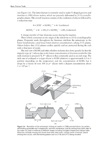
(see Figure 3.6). The latter feature is routinely used to make V-shaped grooves and
trenches in (100) silicon wafers, which are precisely delineated by {111} crystallo-
graphic planes. The overall reaction consists of the oxidation of silicon followed by
a reduction step:
−
(
Si+2 OH → Si OH) 2 ++ +4e − (oxidation )
Si (OH ) ++ + 4e − + 4 H O→ Si (OH ) −− + 2 H (reduction )
2 2 6 2
A charge transfer of four electrons occurs during the reaction.
There is little consensus on the origin of the selectivity to {111} crystallographic
planes. Proposals made throughout the literature attribute the anisotropy to the
lower bond density—and hence lower electron concentration—along {111} planes.
Others believe that {111} planes oxidize quickly and are protected during the etch
with a thin layer of oxide.
The etch rate of KOH and other alkaline etchants also slows greatly for heavily
++
doped p-type (p ) silicon due to the lower concentration of electrons needed for this
etch reaction to proceed [7]. P silicon is thus commonly used as an etch stop. The
++
etch rate of undoped or n-type silicon in KOH solutions is approximately 0.5 to 4
µm/min depending on the temperature and the concentration of KOH, but it
drops by a factor of over 500 in p ++ silicon with a dopant concentration above
−3
1 × 10 cm .
20
{111} <100>
{100}
Self-limiting
etches
Membrane
(a)
{100} Front side mask {100}
{111}
{111}
54.74°
0.707a
a Back side mask {110}
(b)
Figure 3.6 Illustration of the anisotropic etching of cavities in {100}-oriented silicon: (a) cavities,
self-limiting pyramidal and V-shaped pits, and thin membranes; and (b) etching from both sides of
the wafer can yield a multitude of different shapes including hourglass-shaped and oblique holes.
When the vertically moving etch fronts from both sides meet, a sharp corner is formed. Lateral
etching then occurs, with fast-etching planes such as {110} and {411} being revealed.