
Page 73 - An Introduction to Microelectromechanical Systems Engineering
P. 73
52 Processes for Micromachining
nearly vertical, which gives RIE vertical anisotropy. Asymmetric electrodes and low
chamber pressures (5 Pa) are characteristic of RIE operation. Inductively coupled
plasma reactive ion etching (ICP-RIE) provides greater excitation to the electron
cloud by means of an externally applied RF electromagnetic field. Inductively cou-
pled plasma (ICP) increases the density of ions and neutrals resulting in higher etch
rates. The ion bombardment energy is controlled by a separate power supply driving
the platen on which the wafer sits.
A different, purely physical method of etching is ion milling, in which noble-gas
ions (usually argon) are remotely generated, then accelerated at the substrate though
a potential on the order of 1 kV. The directionality of the ions results in a very verti-
cal etch profile. Because a chemical reaction is not required, any material can be
etched by ion milling. The ion-milling rate is typically much slower than with RIE
and varies widely with the material [4].
The remainder of this section focuses on DRIE and its application in
micromachining. Further reading on the basics of plasma etching is suggested at the
end of this chapter.
DRIE
DRIE evolved in the mid 1990s from the need within the micromachining commu-
nity for an etch process capable of vertically etching high-aspect-ratio trenches at
rates substantially larger than the 0.1 to 0.5 µm/min typical of traditional plasma
and RIE etchers. In one approach, developed by Alcatel, the wafer is cooled to cryo-
genic temperatures. Condensation of the reactant gases (SF and O ) protects the
6 2
sidewalls from etching by the reactive fluorine atoms. However, cryogenic cooling
may be difficult to maintain locally and could result in undesirable thermal stresses.
Another approach currently used by Alcatel, PlasmaTherm, and Surface Tech-
nology Systems (STS) [14] follows a method patented by Robert Bosch GmbH, of
Stuttgart, Germany, in which etch and deposition steps alternate in an ICP-RIE sys-
tem [15] (see Table 3.3). The etch part of the cycle, typically lasting 5 to 15s, uses SF ,
6
which supplies highly reactive fluorine radicals, to etch silicon. The etch step has both
vertical and isotropic character, resulting in a slight mask undercut (see Figure 3.12).
In the deposition step, a fluorocarbon polymer (made of a chain of CF groups similar
2
in composition to Teflon™), about 10 nm thick, is plasma-deposited using C F as
4 8
+
the source gas. In the following etch step, the vertically oriented ions (SF ) enhance
x
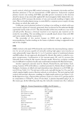
Table 3.3 Process Characteristics of DRIE in the STS System
Etch step 5–15s
SF flow 80–150 sccm
6
Etch power to coil 600–2,500W
Etch power to platen 5–30W
Deposition step 5–12s
C F flow 70–100 sccm
4 8
Deposition power to coil 600–1,500W
Pressure 0.5–4 Pa
Platen temperature 0º–20°C
Etch rate 1–15 µm/min
Sidewall angle 90° ± 2°
Selectivity to photoresist ≥ 40 to 1
Selectivity to SiO 2 ≥ 100 to 1