
Page 78 - An Introduction to Microelectromechanical Systems Engineering
P. 78
Advanced Process Tools 57
clamping fixture holds the aligned wafers in position, separated by thin spacers at
the wafer edges. If desired, the fixture and wafers can be placed in a chamber with
vacuum, inert gas, oxygen, or other controlled atmosphere. The centers of the
wafers are then brought into contact and the spacers removed, allowing the bonded
area to proceed from the wafer center to the edge. The relative misalignment is rou-
tinely less than 5 µm and can be as good as 1 µm. Direct bonding can be repeated to
form thick multiple-wafer stacks, although experience shows that the thicker the
stack becomes, the more difficult it is to achieve good bonding [21].
Grinding, Polishing, and Chemical-Mechanical Polishing
Some applications use a thin layer of silicon (5 to 200 µm) that is fusion-bonded to a
standard-thickness wafer (525 µm for single-side polished or 400 µm for double-
side-polished, 100-mm-diameter wafers), possibly with a layer of oxide between
them. Instead of attempting to silicon-fusion bond such a thin, fragile layer to a
standard-thickness wafer, two standard-thickness wafers are fusion bonded
together, then one side is thinned down to the desired thickness. The thickness
reduction is achieved using grinding and polishing. The wafer stack is mounted on a
rotating table and ground by a diamond-bonded wheel spinning in the opposite
direction. The grinding mechanically abrades silicon and reduces the thickness of
the wafer to near the desired thickness. Hundreds of micrometers can be removed.
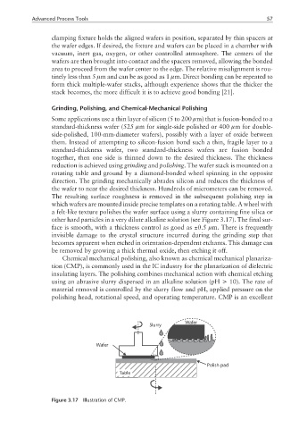
The resulting surface roughness is removed in the subsequent polishing step in
which wafers are mounted inside precise templates on a rotating table. A wheel with
a felt-like texture polishes the wafer surface using a slurry containing fine silica or
other hard particles in a very dilute alkaline solution (see Figure 3.17). The final sur-
face is smooth, with a thickness control as good as ±0.5 µm. There is frequently
invisible damage to the crystal structure incurred during the grinding step that
becomes apparent when etched in orientation-dependent etchants. This damage can
be removed by growing a thick thermal oxide, then etching it off.
Chemical mechanical polishing, also known as chemical mechanical planariza-
tion (CMP), is commonly used in the IC industry for the planarization of dielectric
insulating layers. The polishing combines mechanical action with chemical etching
using an abrasive slurry dispersed in an alkaline solution (pH > 10). The rate of
material removal is controlled by the slurry flow and pH, applied pressure on the
polishing head, rotational speed, and operating temperature. CMP is an excellent
Wafer
Slurry
Wafer
Polish pad
Table
Figure 3.17 Illustration of CMP.