
Page 80 - An Introduction to Microelectromechanical Systems Engineering
P. 80
Advanced Process Tools 59
Table 3.4 Example Solutions for Electroplating Selected Metals
Metal Solution
Gold KAu(CN) :K C H O :HK PO :H O
6
3
2
4
7
2
2
5
NaAuSO :H O
3
2
Copper CuSO :H SO :H O
4
2
2
4
Nickel NiSO :NiCl :H BO :H O
3
2
4
3
2
Permalloy NiSO :NiCl :FeSO :H BO :C H NNaSO :H SO :H O
7
4
4
3
2
3
4
2
3
4
2
Platinum H PtCl :Pb(CH COOH) :H O
2
2
2
2
6
Aluminum LiAlH :AlCl in diethyl ether
3
4
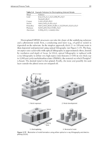
Electroplated MEMS structures can take the shape of the underlying substrate
and a photoresist mold. First, a conducting seed layer (e.g., of gold or nickel) is
deposited on the substrate. In the simplest approach, thick (5- to 100-µm) resist is
then deposited and patterned using optical lithography (see Figure 3.19). The larg-
est aspect ratio achievable with optical lithography is approximately three, limited
by resolution and depth of focus. In LIGA, optical lithography is replaced with
x-ray lithography to define very high aspect ratio features (>100) in very thick (up
to 1,000 µm) poly(methylmethacrylate) (PMMA), the material on which Plexiglas ®
is based. The desired metal is then plated. Finally, the resist and possibly the seed
layer outside the plated areas are stripped off.
UV or x-rays
Mask
Resist
1. Resist exposure 2. Resist development
Metal
Plating
base
3. Electroplating 4. Removal of resist
Figure 3.19 Illustration of mold formation using either optical or x-ray lithography and electro-
plating (LIGA).