
Page 85 - An Introduction to Microelectromechanical Systems Engineering
P. 85
64 Processes for Micromachining
yielding ever lower cost and finer dimensional control. In some applications, such as
ink-jet printer nozzles and automobile fuel-injection nozzles, photolithographic
fabrication methods have been used, but proved less economical than the more
established methods. In addition to competing with lithographic technologies, non-
IC-related fabrication technologies are often used in conjunction with them in the
production of a final product; examples include bulk-micromachined pressure sen-
sors with ultrasonically drilled glass bonded to the back side and ink-jet heads with
surface-micromachined heaters and laser-drilled ports. Two newer techniques for
creating submicrometer patterns are also discussed in this section.
Ultraprecision Mechanical Machining
Cutting tools such as mills, lathes, and drills using a specially hardened cutting edge
have been in use for the production of macroscopic parts for over a century.
Using modern computer-numerical-controlled (CNC) machines with sharply tipped
diamond-cutting tools, many metals and even silicon have been milled to a desired
shape, with some features smaller than 10 µm. Many of these shapes, such as retro-
grade undercuts with flat sidewalls, cannot be formed using lithographic methods.
Resolution of about 0.5 µm can be achieved, with surface roughnesses on the order
of 10 nm [28]. Example applications include optical mirrors and computer hard-
drive disks.
Laser Machining
Focused pulses of radiation, typically 0.1–100 ns in duration, from a high-power
laser can ablate material (explosively remove it as fine particles and vapor) from a
substrate. Incorporating such a laser in a CNC system enables precision laser
machining. Metals, ceramics, silicon, and plastics can be laser machined. Holes as
small as tens of microns in diameter, with aspect ratios greater than 10:1, can be pro-
duced. Arbitrary shapes of varying depths are laser machined by scanning the beam
to remove a shallow layer of material, then scanning again until the desired depth
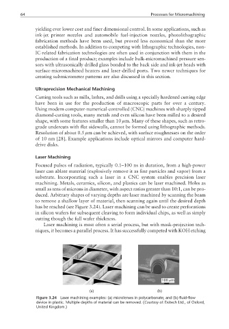
has be reached (see Figure 3.24). Laser machining can be used to create perforations
in silicon wafers for subsequent cleaving to form individual chips, as well as simply
cutting though the full wafer thickness.
Laser machining is most often a serial process, but with mask-projection tech-
niques, it becomes a parallel process. It has successfully competed with KOH etching
Insert here
fig3.24_LaserExamples(a).TIF fig3.24_LaserExamples(b).TIF
µ
100 m
(a) (b)
Figure 3.24 Laser machining examples: (a) microlenses in polycarbonate; and (b) fluid-flow
device in plastic. Multiple depths of material can be removed. (Courtesy of: Exitech Ltd., of Oxford,
United Kingdom.)