
Page 86 - An Introduction to Microelectromechanical Systems Engineering
P. 86
Nonlithographic Microfabrication Technologies 65
and with electroplating in the production of ink-jet nozzles. Due to its speed, low
cost, and rapid turn-around time, laser machining is one of the preferred methods of
creating trenches and cuts in plastics.
Electrodischarge Machining
Electrodischarge machining, also called electrical-discharge machining or sparkero-
sion machining (EDM) uses a series of electrical discharges (sparks) to erode
material from a conductive workpiece. High-voltage pulses, repeated at 50 kHz to
500 kHz, are applied to a conductive electrode, typically made of graphite, brass,
copper, or tungsten. Electrodes as small as 40 µm in diameter have been used, limit-
ing features to about the same size. Features with aspect ratios of over 10 can be fab-
ricated, with a surface roughness on the order of 100 nm. Each discharge removes a
5
3
3
small volume of material, typically in the range of 10 to 10 µm , from the work-
piece [29]. EDM is performed in a dielectric liquid such as mineral oil. Due to heat-
ing, a gas bubble is formed during each voltage pulse. After the pulse, the bubble
collapses, flushing away debris from the blank and electrode.
EDM has been used to create the tooling for molds and stamping tools, as well
as final products such as nozzles and holes in microneedles.
Screen Printing
Screen printing, also known as silk screening, has been used for the printing of
images for millennia. In electronics, it has long been used in the production of
ceramic packages and more recently for large flat-panel displays. In a parallel
process, many ceramic packages are processed together on a single plate, then sepa-
rated near the end of the process. A wide variety of materials, including metals and
ceramics, can be applied using screen printing. It does not have same resolution as
photolithography, but is cost effective and is readily applied to large substrates.
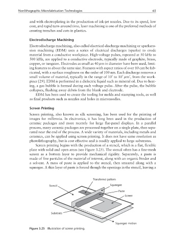
Screen printing begins with the production of a stencil, which is a flat, flexible
plate with solid and open areas (see Figure 3.25). The stencil often has a fine-mesh
screen as a bottom layer to provide mechanical rigidity. Separately, a paste is
made of fine particles of the material of interest, along with an organic binder and
a solvent. A mass of paste is applied to the stencil, then smeared along with a
squeegee. A thin layer of paste is forced though the openings in the stencil, leaving a
Transferred pattern
Stencil Squeegee
Paste
Screen
Substrate
Squeegee motion
Figure 3.25 Illustration of screen printing.