
Page 87 - An Introduction to Microelectromechanical Systems Engineering
P. 87
66 Processes for Micromachining
pattern on the underlying substrate. Drying evaporates the solvent. Firing burns off
the organic binder and sinters the remaining metal or ceramic into a solid, resulting
in a known amount of shrinkage. Metal lines with 125-µm lines and spaces are made
in the production of ceramic packaging (discussed further in Chapter 8) [30], with
30-µm features demonstrated [31]. Film thicknesses after firing range from roughly
10 to 200 µm. Multiple layers of different materials can be stacked.
Microcontact Printing/Soft Lithography
Microcontact printing, a microscale form of ink printing also called soft lithogra-
phy, has been studied by several research groups [32, 33]. It enables low-cost
production of submicrometer patterns and has been studied as an alternative
to conventional photolithography, but is not presently a product fabrication
method.
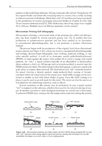
The process begins with the production of the original, hard, three-dimensional
master pattern (see Figure 3.26), which can involve conventional photolithography
and etching, electron-beam lithography, laser scribing, diamond scribing, or any
other suitable method. A mold of an elastomer, usually poly(dimethylsiloxane)
(PDMS), is made against the master, then peeled off to create a stamp with raised
patterns. An “ink,” a liquid solution typically of an alkanethiol (a hydrocarbon
chain ending in a thiol, an –SH group) such as hexadecanethiol, is poured onto the
PDMS stamp and dried. The inked stamp is then held against a substrate coated with
gold, silver, or copper, then removed. The thiol end of each “ink” molecule bonds to
the metal, forming a densely packed, single-molecule-thick coating of hexade-
canethiol where the raised areas of the stamp were. Such SAM coatings can be envi-
sioned as similar to turf with dense blades of grass. Once the SAM coating is in
place, it can be used as an etch mask for the metal. The metal can then be used as an
etch mask for the underlying substrate, such as silicon.
Several variations on this scheme may be performed. In one, a metal catalyst
“ink” is stamped on the substrate, which is then used for the selective plating of cop-
per. In another, proteins or other biological molecules are coated onto a flat stamp.
A patterned PDMS layer contacts the flat stamp and is removed, taking the protein
Hard master mold PDMS stamp “Ink” coating
(a) (b) (c)
Ink monolayer
Metal Etched metal......or...... .Plated metal
(d) (e) (f)
Figure 3.26 Microcontact printing: (a) create master; (b) form PDMS stamp and peel off; (c) coat
with “ink”; (d) press inked stamp against metal and remove, leaving ink monolayer; (e) use self-
assembled monolayer as an etch mask; or (f) as a plating mask.